7 Best PCB Testing Methods for Quality Control?

Reliable PCB quality begins long before a board reaches the customer. It starts with selecting suitable pcb testing methods for the board’s design, materials, and intended operating conditions. A dense six-layer control board may require different checks than a simple single-sided sensor board. Tiny solder bridges, incomplete vias, lifted pads, and intermittent connectors can remain invisible during a quick visual inspection.

Rick Hartley, a respected PCB design educator, has emphasized a practical testing principle: “A good design anticipates how it can fail.” That idea matters on every production line. Testing should not only confirm electrical continuity. It should challenge the board under realistic conditions, including vibration, thermal change, current load, and repeated connection cycles. Automated optical inspection can reveal misplaced components. In-circuit testing can identify resistance, capacitance, and assembly faults. Functional testing shows whether the finished board performs its intended task.

No single method is perfect.

Even a high test-pass rate can hide weak coverage. Fixtures may miss unusual faults. Operators may also trust automated results too quickly. That deserves reflection. Engineers should compare test data with field returns, repair records, and process trends. IPC-based procedures, calibrated instruments, controlled samples, and traceable reports make decisions more reliable. The following seven PCB testing methods explain where each approach fits, what it detects, and where its limitations become visible. Together, they create a stronger quality-control plan without pretending that every defect can be predicted.
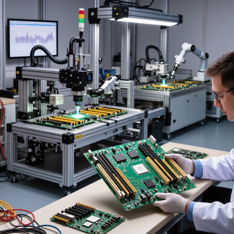
7 Best PCB Testing Methods for Quality Control?

PCB Testing Fundamentals and Quality Control Objectives

PCB Testing Fundamentals and Quality Control Objectives

Reliable PCB testing begins with a clear quality objective: prevent unsafe assemblies from reaching the next process or customer. Inspectors check solder joints, component placement, surface damage, and board cleanliness. These details often reveal process drift before failure appears in the field. The process is not perfect. A clean visual result can still hide an internal void or weak electrical connection.

A balanced control plan uses seven methods: visual inspection, automated optical inspection, X-ray inspection, in-circuit testing, flying-probe testing, functional testing, and boundary-scan testing. Each method answers a different question. Visual inspection finds obvious defects quickly. X-ray examines hidden joints. In-circuit testing checks electrical values and connections. Functional testing confirms whether the assembled board performs its intended task. Engineers should match test depth with product risk, board complexity, and production volume.

Good testing also depends on disciplined records. Teams should trace inspection results, test fixtures, software versions, operator decisions, and sample conditions. Clear acceptance criteria reduce subjective judgments. Calibrated equipment matters. So does training. In practice, technicians sometimes overtrust automated results, while manual reviews may miss repeated patterns. That weakness deserves attention. Reviewing false failures and escapes can improve limits, test coverage, and corrective actions. Quality control becomes stronger when testing is treated as process evidence, not merely a final gate.

Seven Core PCB Testing Methods and Their Operating Principles

7 Best PCB Testing Methods for Quality Control?

Seven methods matter. A 2024 Global Electronics Association outlook valued worldwide electronics production at roughly US$3 trillion. That scale makes measurable PCB quality essential.

Visual inspection checks component orientation, solder shape, scratches, and contamination. Automated optical inspection compares high-resolution images with programmed reference data. It quickly flags missing parts and solder bridges. X-ray inspection penetrates hidden joints, including vias and bottom-terminated packages. IPC-A-610 provides useful acceptance criteria for these visual decisions.

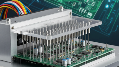
Electrical testing confirms whether copper paths behave correctly. In-circuit testing applies probes to test points and measures resistance, capacitance, continuity, and shorts. Flying-probe testing uses movable probes, reducing fixture costs for small batches. Functional testing powers the assembled board and checks real outputs, such as a stable 5-volt rail or sensor response. Boundary-scan testing shifts patterns through integrated test cells, exposing open connections beneath dense packages. IEEE 1149.1 defines this operating principle.

No single method sees everything. AOI may miss a hidden void, while X-ray may overlook a wrong resistor value. On production floors, test access is often the uncomfortable limitation. NIST measurement guidance stresses traceability, calibration, and uncertainty evaluation. Records should include equipment status, operator identity, limits, and failure images. A failed test is not always a bad board. Sometimes, it reveals a weak program, poor grounding, or an unrealistic threshold. Each result deserves review.

How to Prepare and Perform PCB Tests Step by Step

Preparing and performing PCB tests requires a controlled sequence, not random probing. IPC’s 2024 industry sentiment data showed that quality and reliability remained major manufacturing priorities for most respondents. Begin with the drawing, bill of materials, revision level, and acceptance criteria. Clean the board and inspect solder joints under magnification. Small defects matter.

Use seven complementary methods:

visual inspection, automated optical inspection, X-ray inspection, in-circuit testing, flying-probe testing, functional testing, and boundary-scan testing.

Prepare test points before assembly. Confirm fixture contact, probe pressure, grounding, and software limits. For dense boards, X-ray testing can reveal hidden voids or solder bridges. For prototypes, flying-probe testing often reduces fixture preparation time. The right method depends on volume, access, and failure risk.

Run continuity and isolation checks before applying power. Then test resistance, polarity, signal paths, and programmed functions.
Record voltage, temperature, operator, equipment identification, and test time.

NIST measurement guidance stresses traceability and uncertainty control, so calibration records should remain with every test batch. I still recommend a second review of failed boards.

A false failure is possible. So is a missed intermittent fault. Reinspect suspicious joints, repeat the test, and compare results with a known-good board. Scrap decisions should follow evidence, not pressure.

Comparing PCB Test Methods by Accuracy, Cost, and Coverage

PCB testing is not a single checkpoint.

Seven common methods are visual inspection, automated optical inspection, in-circuit testing, flying-probe testing, functional testing, boundary-scan testing, and X-ray inspection.

Each method measures a different risk. Visual inspection is inexpensive and fast, but it can miss hidden solder joints.

Automated optical inspection improves repeatability, especially for visible placement and solder defects. X-ray inspection reaches concealed connections, although equipment and operation costs are higher.

Accuracy depends on the defect type, not only the machine.

In-circuit testing can locate opens, shorts, and component-value errors with strong precision. It requires dedicated fixtures, which increases setup costs.

Flying-probe testing avoids expensive fixtures and suits prototypes or small batches. It is flexible, but slower during high-volume production.

Functional testing checks whether the assembled board performs its intended task. Coverage is practical, yet diagnosis may be less specific when several faults create the same symptom.

Use layered testing.

A cost-conscious line may combine visual inspection, optical inspection, and sampling-based functional tests. High-density boards may need X-ray or boundary-scan coverage for hidden and programmable devices.

No method is perfect. A clean optical image does not prove electrical reliability, and a passed functional test may overlook gradual solder weakness.

Engineers should review field returns, false failures, test escape rates, and fixture maintenance.

One difficult truth remains: the cheapest test plan can become expensive when coverage gaps reach customers.

Using Test Results to Improve PCB Quality and Reliability

7 Best PCB Testing Methods for Quality Control

Using Test Results to Improve PCB Quality and Reliability

Reliable PCB quality control begins with evidence, not assumptions. Visual inspection can reveal solder bridges, lifted pads, and damaged traces. Automated optical inspection adds consistent image-based checks. In-circuit testing then measures component values, opens, and shorts. Flying-probe testing helps investigate prototypes and small production runs without custom fixtures.

Each method produces different evidence. Boundary-scan testing can expose connection faults between digital devices. Functional testing checks whether the assembled board performs its intended task. X-ray inspection reveals hidden voids, weak joints, and misaligned components beneath packages. The strongest programs compare these results instead of trusting one test alone.

Patterns matter.

A rising solder-bridge rate may indicate stencil wear or excessive paste volume. Repeated open circuits near one connector can point to fixture pressure or handling damage. Engineers should record defect location, test conditions, operator notes, and repair results. This creates a traceable quality history and supports targeted process changes.

Test data should also guide reliability decisions. Boards that pass functional testing may still contain marginal joints or excessive thermal stress. Sampling repaired boards with X-ray or cross-section analysis can expose hidden weaknesses. However, test limits are never perfect. A threshold set too tightly may reject usable boards, while a loose limit can hide early failures. Reviewing false rejects and field returns helps refine limits, inspection frequency, and corrective actions. That review is sometimes uncomfortable, but it prevents confidence from replacing proof.

7 Best PCB Testing Methods for Quality Control

Comparison of the typical fault categories that each PCB test method can identify. Combining visual, electrical, structural, and functional tests improves defect coverage and long-term reliability.

The benchmark counts common fault categories such as missing or misplaced components, solder defects, open circuits, short circuits, incorrect component values, hidden solder-joint defects, and functional failures. Actual coverage varies by board design, equipment, fixtures, and test programming.

Go to Top