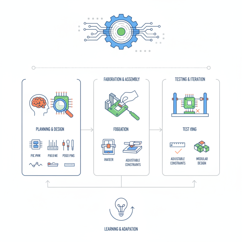
Building a PCB test jig is essential for effective testing and prototyping. This tool can streamline the validation of your printed circuit boards. A well-designed jig allows for faster identification of faults and improves overall product quality.
Creating a PCB test jig is not straightforward. It requires careful planning and understanding of circuit requirements. You must consider component placement, connection types, and signal integrity. Mistakes made in the design phase can lead to testing errors. Experimenting with different configurations helps refine your approach.
Incorporating features like adjustable constraints and modular design can enhance functionality. However, simplification often introduces its own challenges. A balance is necessary between complexity and usability. Reflecting on past prototypes can provide valuable insights. Building an effective PCB test jig is a journey of learning and adaptation.
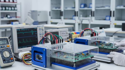
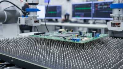
Understanding PCB test jigs is crucial in modern prototyping. These jigs provide a reliable method for testing printed circuit boards (PCBs) before mass production. A recent industry report highlighted that effective testing can increase product quality by up to 30%. This data signifies the importance of integrating test jigs into the development process.
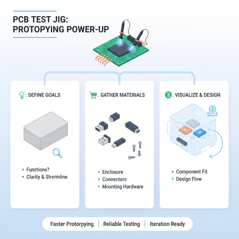
PCB test jigs streamline the testing phase, reducing production time and costs. They allow for simultaneous testing of multiple boards, which can enhance efficiency. However, building an optimal test jig can be challenging. Developers often overlook the necessity of precise alignment and secure connections. Misalignments can lead to inaccurate readings during tests.
Tips: Ensure your jig design includes adjustable components. This flexibility accommodates various PCB sizes. Regularly revisit your design after initial tests. Reflect on what worked and what didn’t. Sometimes, minor adjustments can lead to significant improvements. Don't hesitate to iterate. Embrace imperfections as part of the learning process.
Building a PCB test jig requires careful consideration of essential components. At the core of this construction are fixtures, connectors, and testing interfaces. Fixtures help stabilize the PCB during testing. They must be tailored to the board’s size and shape. Connectors facilitate reliable electrical connections. They should match the PCB’s specifications exactly.
Incorporating a programmable power supply adds versatility. This allows for various voltage and current tests. Additionally, using high-precision multimeters ensures accurate measurements. According to industry data, 70% of test failures occur due to poor connector management. Therefore, attention to these components is critical.
Tips: Always validate your connections before testing. This can save time and resources. Regularly check your fixtures for any wear or damage. A minor oversight here can lead to inaccurate results. Pay attention to thermal conditions. Overheating can affect both components and tests.
Lastly, remember that prototyping often reveals flaws. Evaluate your design frequently. This ongoing reflection enhances the jig's efficacy. Building a test jig can be a complex task, but the right components are crucial for achieving reliable results.
Designing a PCB test jig can significantly improve your prototyping phase. Start by defining the goals of your test jig. What functions do you need to test? This clarity helps streamline the design process. Gather the essential materials, such as a suitable enclosure, connectors, and mounting hardware. It’s crucial to visualize how these components will fit together.
Once assembled, it’s time for wiring. Clear and organized connections are vital. Messy wiring can lead to errors and frustration. Plan a layout that minimizes interference and allows for easy modifications later. Remember that mistakes will happen. Perhaps a wrong connection or an oversight in planning. Reflect on these moments; they are valuable learning opportunities.
After completing your test jig, conduct initial tests. Check for basic functionality and refine as needed. The first iteration won’t be perfect. You may find inefficiencies or untested scenarios. Document these insights for future projects. Continuous improvement is part of the design journey. Your PCB test jig should evolve as you learn from testing.
When evaluating printed circuit boards (PCBs), effective testing methods are essential for quality assurance. The use of automated test equipment (ATE) has risen significantly. A report by IPC shows that 45% of manufacturers utilize ATE to streamline their testing process. This method enhances precision and minimizes human error. Efficient testing techniques include boundary scan testing and in-circuit testing (ICT), which are crucial for detecting faults early.
Another common method is functional testing. This technique assesses whether the assembled PCB performs its intended functions. It's critical to implement this after initial production. Around 60% of firms report that functional testing significantly reduces long-term defects. However, it requires clear protocols and skilled personnel, which can be challenging to maintain.
Data from a recent study indicates that 70% of PCB failures occur due to design issues. This highlights the need for continuous feedback during testing. Any inefficiencies in the testing process not only prolong development but also increase costs. An iterative approach can help identify failures earlier. Adapting testing methods based on prior results allows for ongoing improvements, ensuring better reliability in future designs.
Testing PCBs can be tricky. Common issues often arise during the process. One frequent problem is insufficient power supply. Make sure your test jig provides the correct voltage. A mismatch can lead to unreliable results. It's essential to double-check your power connections.
Another common issue is intermittent connections. Poor soldering might cause components to fail. Inspect the solder joints carefully, ensuring each connection is stable. Sometimes, visual inspection is not enough. Use a multimeter to test continuity on critical paths.
Calibration errors can also impact test accuracy. Regularly calibrate your equipment to ensure reliable readings. It's easy to overlook this step, but it can save time in the long run. Reflect on your testing procedures often. Continuous improvement is vital.
| Issue | Description | Possible Causes | Troubleshooting Steps |
|---|---|---|---|
| No Power | The test jig shows no signs of power when turned on. | Faulty power supply, loose connections, or damaged components. | Check power supply voltage, inspect connections, and test components. |
| Incorrect Readings | Measurements from the jig do not match expected values. | Calibration issues, component failure, or incorrect setups. | Recalibrate the equipment and check component values. |
| Intermittent Connections | Connections are non-consistent, affecting the testing results. | Worn-out connectors, damaged PCB traces, or dirty contacts. | Inspect and replace connectors, clean contacts and check traces. |
| Overheating | Test jig components heat up excessively during operation. | Insufficient cooling, overloading components or design flaws. | Improve ventilation, check load levels, and redesign if necessary. |
| Inconsistent Test Results | Tests yield different results on repeated trials. | Variability in conditions, user error, or equipment malfunction. | Standardize testing conditions, ensure proper technique, check equipment. |