How to Choose the Right Pogo Pins for Your PCB Design Needs
In the rapidly evolving landscape of electronics, the choice of components for PCB (Printed Circuit Board) design has become increasingly critical. Among these components, pogo pins have garnered significant attention due to their unique attributes, which facilitate reliable and efficient connectivity in various applications. According to a recent industry report, the global market for pogo pins is projected to grow at a CAGR of 5.3%, highlighting the rising demand for high-quality electrical connections in sectors ranging from consumer electronics to medical devices. As engineers and designers seek innovative solutions for their PCB needs, understanding how to select the right pogo pins becomes paramount.
The selection of pogo pins for PCB design involves careful consideration of factors such as force requirements, cycle life, and the environment in which they will operate. Analyzing specifications and performance characteristics is essential to ensure optimal functionality. Industry insights suggest that improper selection can lead to increased failure rates, which, according to another report, can cost manufacturers up to 10% of their total production expenses. Therefore, knowing how to choose the appropriate pogo pins for a PCB is essential not only for enhancing the reliability of electronic devices but also for maintaining cost efficiency in production.

Understanding the Functionality of Pogo Pins in PCB Designs
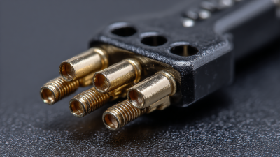
Pogo pins, also known as spring-loaded pins, are essential components in PCB designs, facilitating reliable electrical connections. They are particularly used in applications where a temporary connection is required, such as in test fixtures, programming interfaces, and docking stations. Understanding their functionality is crucial for designers who wish to ensure that their PCBs maintain high reliability and efficiency under various operating conditions.
The working principle of pogo pins revolves around a spring mechanism that allows for compression and extension, providing a stable contact with the pads on the PCB. This feature enables the pins to adapt to different board thicknesses and surface variances, which can be common in high-density designs. Additionally, their design often includes a gold or nickel plating, which enhances conductivity and reduces oxidation, thereby improving the longevity and performance of the connection. Properly implemented, pogo pins can significantly streamline the assembly process and provide a robust solution for creating test and diagnostic interfaces.
Understanding the Functionality of Pogo Pins in PCB Designs
Key Specifications to Consider When Selecting Pogo Pins
When selecting pogo pins for your PCB design needs, it's essential to consider several key specifications that can significantly impact performance and reliability. One of the primary factors is the pin's diameter and length. A thicker pin may offer better conductivity and durability, while the length needs to be appropriate for the intended application, ensuring a secure connection without unnecessary stress on the PCB. Additionally, the spring force should be evaluated to ensure the pins can maintain proper contact throughout their lifecycle.
Another important specification is the plating material of the pogo pins. Depending on the environment and application, different materials (such as gold, nickel, or even alloy coatings) may provide varying levels of corrosion resistance and conductivity. For instance, gold plating is highly conductive and resistant to oxidation, making it ideal for high-frequency applications, while nickel can be a cost-effective alternative for less demanding environments.
Tips: Always prototype your design with various pin configurations to test for optimal performance in real conditions. Additionally, consider the manufacturing tolerances and ensure that your chosen pogo pins can be easily integrated with your PCB layout. It's advisable to consult technical datasheets and engineering guidelines to match specifications with your specific application needs.
Assessing Pogo Pin Durability and Material Composition
When selecting pogo pins for PCB design, it is crucial to evaluate their durability and material composition, as these factors significantly impact performance and longevity. Pogo pins are typically made from a variety of metals including spring steel, gold, and nickel plating, each offering different degrees of conductivity, corrosion resistance, and mechanical properties. Choosing a high-quality material can enhance the electrical connection while ensuring resilience against wear and fatigue over prolonged use. For instance, gold plating is commonly preferred for its excellent conductivity and resistance to oxidation, making it ideal for high-frequency applications.
Furthermore, the durability of pogo pins is influenced by their mechanical design, including spring force and lifespan ratings. A properly designed pogo pin should withstand numerous mating cycles without degradation. Testing methods such as cyclic loading can help in determining the expected lifespan and operational reliability under specific conditions. It is essential to align these specifications with the intended application to ensure optimal performance, as certain designs may excel in standard environments while struggling under extreme conditions. Hence, assessing both material composition and durability will ultimately lead to a well-informed choice that meets the unique demands of each PCB design project.
Analyzing the Importance of Pogo Pin Pitch and Configuration
When designing printed circuit boards (PCBs), the selection of pogo pins can significantly impact the reliability and performance of the final product. One of the most critical factors to consider is the pitch and configuration of the pogo pins. According to a recent industry report, optimal pogo pin pitch is often within the range of 0.5mm to 2.0mm, depending on the application and density of the connection points. Choosing the right pitch ensures effective alignment and minimizes the risk of misalignment during testing phases.
Additionally, the configuration of pogo pins plays a vital role in achieving consistent performance. Configuring pogo pins in a staggered or structured setup can improve contact reliability. Research highlights that a staggered arrangement can better distribute forces and reduce wear over time, especially in high-cycle applications. Implementing such configurations not only enhances mechanical stability but also ensures a lower resistance to electrical signals.
**Tip:** Always consider the specific requirements of your PCB layout when selecting pogo pin pitch to avoid potential misalignment issues.
**Tip:** Assess the testing cycles and environmental conditions to determine the most suitable pogo pin configuration, which can lead to improved longevity and effectiveness during testing.
How to Choose the Right Pogo Pins for Your PCB Design Needs - Analyzing the Importance of Pogo Pin Pitch and Configuration
| Pin Type |
Pitch (mm) |
Configuration |
Max Current (mA) |
Applications |
| Standard |
2.54 |
Single Row |
300 |
Test Fixtures, Prototyping |
| High-Density |
1.27 |
Dual Row |
200 |
Mobile Devices, IoT Sensors |
| Low Profile |
1.00 |
Single Row |
150 |
Wearable Tech, Compact PCBs |
| Heavy Duty |
3.00 |
Single Row |
500 |
Test Equipment, Industrial Robotics |
| Ultra-Fine |
0.5 |
Array |
50 |
Micro Electronics, Advanced Cameras |
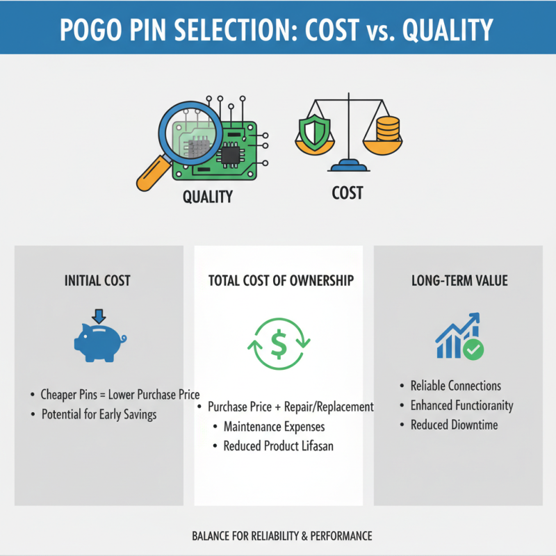
Evaluating Cost-Effectiveness in Pogo Pin Selection for PCB Applications
When evaluating cost-effectiveness in the selection of pogo pins for PCB applications, it is essential to balance quality and budgetary constraints. Pogo pins are critical components that facilitate reliable electrical connections in numerous electronic devices. Therefore, the initial cost-saving from opting for cheaper pins might lead to increased maintenance costs or reduced functionality over the product lifecycle. Analyzing the total cost of ownership, which incorporates not only the purchase price but also potential repair and replacement expenses, is fundamental in making informed decisions.
Another vital aspect to consider is the specific application and environmental conditions the pogo pins will face. Factors such as the required durability, conductivity, and resistance to wear can significantly influence cost. Investing in higher-quality pogo pins might mitigate failures that could arise from subpar alternatives, ultimately reducing operational interruptions and enhancing product longevity. By carefully assessing the long-term benefits of durability and reliability against initial expenditure, designers can ensure their PCB applications remain both effective and economical, meeting both technical and financial requirements.