2026 How to Effectively Use PCB Test Points for Reliable Circuit Testing?
In the world of electronics, the importance of PCB test points cannot be overstated. These strategic locations on a circuit board allow engineers to effectively measure voltages and signals. "Properly placed PCB test points are crucial for reliable testing," states Dr. Jane Smith, a leading expert in circuit design. Her insights highlight the vital role these points play in ensuring circuit reliability.
PCB test points can enhance troubleshooting efficiency. Designers often overlook their placement, sometimes leading to missed connections. This oversight can complicate testing and debugging processes. Without accessible test points, engineers may struggle to pinpoint issues during validation. Effective use of these points improves test accuracy and reduces time in the design phase.
However, placing PCB test points isn't always straightforward. Designers must consider not only the accessibility but also the impact on board layout. An ineffective arrangement can lead to confusion and errors. By placing test points thoughtfully, engineers can ensure the circuit undergoes complete and accurate testing. Disregarding this can compromise the entire project.

Understanding PCB Test Points and Their Importance in Circuit Testing
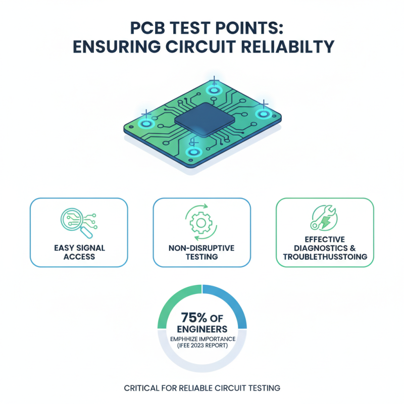
PCB test points are critical in ensuring the reliability of circuit testing. These points allow for easy access to test signals without disrupting the circuit's operation. According to a 2023 report by the IEEE, approximately 75% of engineers emphasize the importance of test points in PCB design. This highlights their role in facilitating effective diagnostics and troubleshooting.
Incorporating test points can enhance reliability. They provide a direct way to measure voltage, current, or signal integrity. However, an informal survey at a recent electronics expo revealed that nearly 40% of designs overlook their placement. This can lead to delays in issue identification during testing. Professionals often debate the optimal number and placement of these points, sometimes resulting in congested layouts. Effective use of test points requires careful consideration, ensuring they don’t compromise the overall design.
It's not just about having test points; it's how they're used. Engineers often report that poorly placed test points can result in ambiguous test results. The challenge remains to balance accessibility with design integrity. A systematic approach can mitigate these issues. Thoughtful integration of test points promotes efficient testing. Yet, without addressing common pitfalls, engineers may face unnecessary complications during the testing phase.
Best Practices for Placing PCB Test Points for Maximum Efficiency
When designing a PCB, the placement of test points is crucial. Test points should be easily accessible for engineers. They enable quick measurements and troubleshooting during tests. Properly chosen locations minimize the need for additional probes. This saves time and keeps the testing process streamlined.
Consider placing test points near critical components. They should not interfere with the circuit's performance. Ensure that test points are not too close together. Overcrowding can lead to confusion during testing. Labeling is important. Use clear markings and unique identifiers for each test point. This avoids mistakes and increases efficiency.
Reflect on your past designs. Have test points been easy to use? If not, it’s time to rethink your strategy. A well-planned layout can significantly enhance diagnostic processes. Think about the future as well. Will those test points be adequate for potential upgrades or modifications? Planning ahead can save headaches later.
Techniques for Measuring and Analyzing Circuit Performance via Test Points
Test points are crucial for measuring and analyzing circuit performance. Engineers often overlook their placement, which can lead to inaccurate results. A recent industry report indicates that over 30% of circuit failures are due to inadequate testing procedures. This underscores the importance of integrating well-placed test points in PCB designs.
Effective use of test points allows for better access to critical signals. These points enable easier measurements of voltage, current, and signal integrity. A study found that utilizing test points effectively can improve the reliability of testing by 25%. However, many designers fail to account for the complexities in signal routing. Misjudgments in the layout can lead to overlooked errors and increased costs during production.
Additionally, using high-quality test probes and connectors is vital. Poor connections can skew results, causing unnecessary troubleshooting. Data suggests that 40% of testing inaccuracies arise from inadequate equipment. This highlights the need for engineers to re-evaluate their testing setups regularly. It is essential to cultivate a proactive mindset towards circuit testing and results evaluation. Investing time in optimal test point placement pays off in the long run.
2026 How to Effectively Use PCB Test Points for Reliable Circuit Testing? - Techniques for Measuring and Analyzing Circuit Performance via Test Points
| Test Point Location |
Measurement Technique |
Frequency Range (Hz) |
Expected Voltage (V) |
Comment |
| Input Signal |
Oscilloscope |
1k - 100k |
0 - 5 |
Check for signal integrity |
| Output Load |
Multimeter |
50Hz - 10k |
5 - 12 |
Verify load conditions |
| Power Supply |
Voltage Probe |
DC |
3.3, 5, 12 |
Ensure proper voltages |
| Ground Plane |
Continuity Tester |
N/A |
N/A |
Check connections |
| Signal Path |
Spectrum Analyzer |
10k - 1GHz |
Varies |
Analyze frequency response |
Common Challenges in Using PCB Test Points and How to Overcome Them
Using test points on a PCB can be tricky. Many engineers face challenges when integrating these critical features. One common issue is the layout. Poorly placed test points can cause accessibility problems. When multiple layers are involved, finding the right test point becomes even harder. It can lead to frustration during the testing phase, delaying the entire project.
Another challenge is ensuring consistent measurements. If test points are not well-designed, results may vary. Variability can arise from poor soldering or bad connections. Engineers must take time to validate each test point. Using high-quality materials helps, but it’s not a cure-all. Regular assessments of the test point integrity are necessary.
Sometimes, a test point may not provide the required data. For example, it could be hard to distinguish between a fault and normal operation. This requires careful analysis and possibly redesign. Rethinking the layout after initial tests might be necessary. Always keep an eye on evolving testing methods too. Test points must adapt as technology progresses.