10 Essential Tips for Designing an Effective PCB Test Jig
The design and implementation of an effective PCB test jig is a critical component in the electronics manufacturing sector, contributing significantly to quality assurance and product reliability. According to a recent report by the Electronics Industry Association, approximately 30% of manufacturing defects can be attributed to inadequate testing and validation processes. A well-designed test jig not only streamlines the testing process but also enhances the overall productivity of electronic devices, making it an indispensable tool for engineers and manufacturers alike.
Expert insights reveal the significance of precision in designing PCB test jigs. Dr. Alex Thompson, a leading authority in PCB test technology, states, "An effective test jig serves as the backbone of any testing process; it ensures that we are not just identifying faulty boards but also continuously improving our manufacturing protocols." This underscores the necessity for engineers to prioritize the design of test jigs that are not only functional but also adaptable to various testing requirements.
In light of these considerations, this article provides ten essential tips for designing an effective PCB test jig, aiming to guide engineers in enhancing their testing frameworks. By leveraging best practices and expert knowledge, the goal is to mitigate defects and elevate the standards of electronic manufacturing through the strategic application of PCB test jigs.

Understanding the Purpose of a PCB Test Jig
A PCB test jig is an essential tool in the manufacturing and development of printed circuit boards (PCBs).
Its primary purpose is to facilitate the testing and validation of PCB functionality throughout the production process.
By providing a stable and repeatable platform, a test jig allows engineers and technicians to assess individual components,
trace connections, and overall board performance efficiently.
The jig’s design enables it to interface with testing equipment, ensuring that every PCB is subjected to the same rigorous evaluations.
Furthermore, understanding the purpose of a PCB test jig extends beyond mere functionality;
it also plays a critical role in quality assurance.
By identifying faults or discrepancies early in the production cycle, manufacturers can prevent defective boards from reaching the market,
thereby reducing costs and enhancing reliability. Additionally, the jig can be tailored to accommodate different testing requirements,
whether it be for simple continuity checks or more complex signal integrity measurements.
Ultimately, the effectiveness of a PCB test jig hinges on its ability to provide precise and
repeatable results, helping to ensure that every circuit board meets the required specifications and performs as intended.
Key Design Considerations for PCB Test Jigs
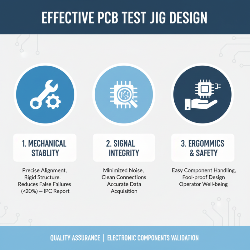
When designing an effective PCB test jig, several key considerations can greatly influence the validation and quality assurance process of electronic components. One of the foremost factors is the jig's mechanical stability. According to a report by the IPC (Institute of Printed Circuits), mechanical failures during testing can lead to a significant increase in the false failure rates, sometimes exceeding 20%. Ensuring that the jig maintains precise alignment and rigidity under testing conditions is vital to obtaining accurate and reproducible results.
Another critical design aspect is the electrical connectivity within the test jig. The choice of appropriate test probes and connectors can impact the integrity of the signals being transmitted during testing. Data from the IEEE indicates that up to 35% of test failures can be traced back to inadequate contact or resistance issues during testing. Thus, incorporating high-quality materials and components ensures reliable connections and minimizes signal loss. Additionally, implementing appropriate shielding and grounding techniques can mitigate noise interference, further enhancing the performance and accuracy of the test jig.
Lastly, effective thermal management within the test jig cannot be overlooked. Research indicates that temperature fluctuations can adversely affect electronic components, leading to erroneous test results. A study published in the Journal of Electronic Testing showed that maintaining a controlled temperature environment can improve the accuracy of testing by up to 15%. By integrating cooling solutions and using temperature-stable materials, designers can enhance the reliability of their PCB test jigs.
Essential Components to Include in Your PCB Test Jig
When designing an effective PCB test jig, it is crucial to incorporate essential components that facilitate thorough and reliable testing. One of the core components is the test pins, which serve as electrical contact points with the PCB. According to industry reports, improper contact with test pins can lead to a staggering 30% increase in test failures, highlighting the need for high-quality, precision-engineered pins that align perfectly with the PCB pads for accurate measurements.
Another vital component is the fixture, which holds the PCB securely in place during testing. A report by IPC (Institute of Printed Circuits) emphasizes that a well-designed fixture can significantly reduce test time and improve overall testing efficiency by up to 25%. This is achieved through proper alignment and stability, which prevents movement that could lead to erroneous test results.
Additionally, integrating a programmable logic controller (PLC) can streamline the testing process, enabling automated adjustments based on real-time feedback from the test results, thus further enhancing test precision and reliability.
To ensure comprehensive testing, incorporating various test strategies such as boundary scan, in-circuit testing (ICT), and functional testing modules within your test jig is essential. These methodologies not only detect different types of faults but also ensure that the PCB operates correctly under various conditions.
By addressing these key components and strategies, engineers can significantly enhance the effectiveness of their PCB test jigs and ensure high-quality outputs.
Best Practices for Ensuring Accurate Test Results
When designing an effective PCB test jig, ensuring accurate test results hinges on several best practices that contribute to the reliability and reproducibility of the testing process.
First and foremost, the jig should be constructed with precise alignment features that ensure the PCB is held securely in the correct position throughout testing. This minimizes the risk of misalignment caused by thermal expansion or mechanical disturbances, which can lead to inconsistent test outputs.
Additionally, employing high-quality connectors and test points will help reduce contact resistance and improve signal integrity during measurements.
Another crucial aspect is to limit noise and interference within the testing environment. Implementing shielding and proper grounding for the jig can significantly enhance the accuracy of test results.
It is also beneficial to incorporate automated test sequences that standardize the testing process, reducing human error and variability between tests. Furthermore, utilizing well-calibrated and validated test equipment will further strengthen the reliability of the results obtained.
By focusing on these core practices, engineers can create a robust PCB test jig that delivers accurate and dependable testing outcomes.
Tips for Improving Usability and Maintenance of Test Jigs
When designing a PCB test jig, enhancing usability and maintenance can significantly improve the testing process. First, consider the user interface and ergonomics of the jig. An intuitive layout, with clearly labeled ports and controls, allows operators to quickly familiarize themselves with the equipment. Incorporating features like adjustable mounting brackets and easy-access components can minimize downtime during setup and reduce the risk of user error. Additionally, ensuring that all connections are robust and clearly marked prevents confusion, making it easier for users to perform tests efficiently.
Maintenance is another critical aspect of a test jig's design. To facilitate regular upkeep, use modular components that can be easily replaced or serviced. This not only extends the lifespan of the jig but also reduces the time and effort required to perform maintenance tasks. Implementing features such as status indicators for component health and suggestions for troubleshooting can empower users to handle minor issues independently. Providing comprehensive documentation and guides, both in physical form and digitally, will further support maintenance efforts, ensuring the jig remains in optimal condition and maximizing its usability over time.
10 Essential Tips for Designing an Effective PCB Test Jig
| Tip Number |
Tip |
Description |
Usability Improvement |
Maintenance Consideration |
| 1 |
Modular Design |
Create a test jig that can easily be modified for different PCBs. |
Allows for quick adaptation to various designs. |
Facilitates easier upgrades and component replacements. |
| 2 |
Clear Labeling |
Label all components and test points clearly. |
Improves user understanding and reduces errors. |
Ease of maintenance and troubleshooting. |
| 3 |
Use of Standardized Connectors |
Employ standard connectors to ease the setup process. |
Familiar interfaces for users improve speed of setup. |
Simplifies the replacement of connectors. |
| 4 |
Accessibility |
Ensure all test points are easily accessible. |
Saves time during testing and maintenance. |
Reduces strain on users, ensuring safety. |
| 5 |
Robust Design |
Construct the jig to withstand frequent usage. |
Increases reliability during tests. |
Lowers maintenance costs over time. |
| 6 |
Power Management |
Incorporate smart power management features. |
Maximizes efficiency during testing. |
Helps in reducing heat generation and prolongs life. |
| 7 |
User Training |
Provide training for all users of the test jig. |
Ensures consistent and correct usage. |
Reduces errors and increases efficiency. |
| 8 |
Feedback Mechanism |
Include a way for users to give feedback on the jig. |
Helps in continual improvement of design. |
Informs updates for maintenance procedures. |
| 9 |
Regular Checks |
Schedule regular maintenance checks of the jig. |
Ensures continuous reliability during tests. |
Proactive approach helps minimize down time. |
| 10 |
Documentation |
Keep comprehensive documentation of the test jig. |
Aids in training and operation. |
Simplifies the troubleshooting and repair processes. |