Essential Tips for Effective Wafer Testing Explained
Wafer testing is a critical process in semiconductor manufacturing. It involves assessing the performance and reliability of silicon wafers. According to Dr. Emily Chen, a leading expert in wafer testing, “Effective wafer testing can save time and resources while ensuring product quality.” Her insight underscores the importance of having a robust testing strategy.
The testing phase often reveals unexpected issues that could derail a project. For example, minor defects can lead to significant failures later in production. Engineers must analyze results carefully to identify root causes. Many times, results may be inconclusive, requiring further investigation.
Additionally, sometimes testing methods themselves need improvement. It’s essential to stay updated with the latest technologies. Not every approach works perfectly every time, and adaptation is key. Continuous learning and adjustment in wafer testing can lead to more effective outcomes. Embracing this mindset will elevate the overall quality of semiconductor products.

Introduction to Wafer Testing and Its Importance
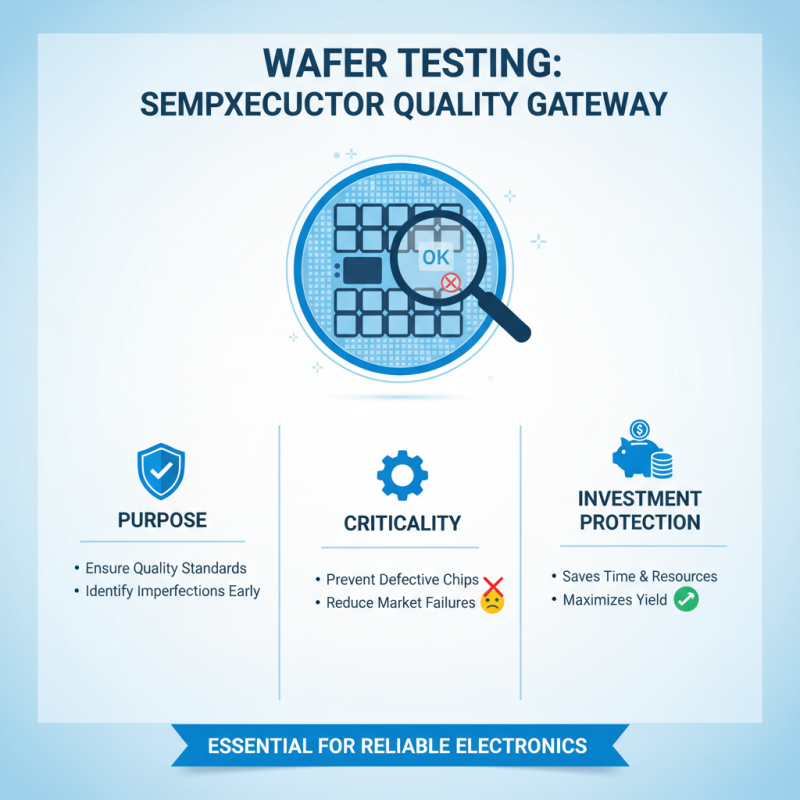
Wafer testing plays a crucial role in the semiconductor manufacturing process. It ensures that every wafer meets rigorous quality standards. This stage is critical because imperfections can lead to defective chips. When we overlook wafer testing, we increase the risk of malfunctioning products reaching the market. Each wafer represents significant investment, both in time and resources.
Understanding wafer testing involves delving into several methods used to evaluate wafers. These methods focus on electrical performance and structural integrity. Often, testing can reveal inconsistencies that may not be visible at first glance. It's essential to analyze yield rates and identify potential failure points. Sometimes, we might find ourselves relying too much on automated systems for testing, which can foster complacency.
A common challenge in wafer testing is balancing efficiency and thoroughness. Rushing through tests can lead to missed defects. It's essential to cultivate a mindset that prioritizes careful analysis over speed. Incorporating more manual checks may slow production but can improve overall quality. Ultimately, achieving a balance between these factors leads to better outcomes. We need to always reassess our methods and strive for improvement.
Key Factors Influencing Wafer Testing Effectiveness
Wafer testing is critical for ensuring the quality of semiconductor devices. Several key factors significantly influence its effectiveness. One major aspect is the equipment used during testing. The precision and calibration of the testing instruments play a huge role. Any discrepancies can lead to inaccurate results, which may affect the entire production line.
Environmental conditions also matter. Temperature swings and humidity can alter the behavior of wafers. Such variations can lead to flawed readings. It’s essential to maintain a controlled environment for testing. A cleanroom with regulated conditions ensures that contaminants do not affect the test outcomes.
Another area for reflection is personnel training. Test operators should have comprehensive training. Even skilled technicians can overlook details, leading to potential issues. Regular workshops and technique refreshers can help. Testing procedures must be followed carefully to avoid errors. Consistent evaluation of both processes and personnel is needed for ongoing improvement.
Essential Tips for Effective Wafer Testing Explained - Key Factors Influencing Wafer Testing Effectiveness
| Testing Factor |
Impact on Effectiveness |
Recommended Practices |
| Probe Positioning |
Critical for accurate measurements |
Use automated systems for consistency |
| Environmental Control |
Affects test results and yield |
Regulate temperature and humidity |
| Test Equipment Calibration |
Ensures accuracy of readings |
Regularly verify equipment settings |
| Data Analysis Techniques |
Influences defect detection |
Utilize advanced statistical methods |
| Test Duration |
Longer tests may catch more issues |
Balance between time and thoroughness |
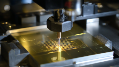
Step-by-Step Process of Conducting Wafer Tests
Conducting wafer tests requires meticulous attention to detail. Each wafer undergoes a step-by-step process, starting with visual inspection. This initial check identifies any obvious defects, such as cracks or discoloration. According to a recent report, up to 20% of wafers can be rejected at this stage alone.
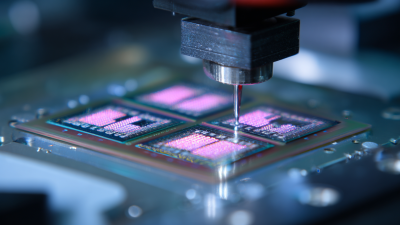
After visual inspection, electrical testing is essential. This phase checks the performance of the circuits. Parameters like resistance and capacitance are measured to ensure functionality. The industry standard indicates that nearly 95% of manufacturing defects are detected during this testing phase. However, issues can be missed if testers aren’t careful.
Thermal tests follow to assess performance under varying temperatures. This can uncover reliability issues that may not surface during electrical tests. Surprisingly, 15% of chips can fail during this phase. Each failure can lead to costly production setbacks. Reflecting on these outcomes, improving precision in testing methods remains a challenge for engineers. Continuous training and updated tools are crucial for progress.
Common Challenges Faced During Wafer Testing
Wafer testing can be a complex process. Various challenges often hinder effective outcomes. One significant issue is the presence of defects on the wafer. These defects can arise during manufacturing, leading to inaccurate test results. Sometimes, the testing equipment may not be calibrated correctly. This miscalibration can cause false failures or missed defects.
Another common challenge is the time constraint during testing. Engineers may rush through the process, leading to oversight. This pressure can compromise the quality of testing. Additionally, environmental factors such as temperature fluctuations can impact test accuracy. Handling wafers in less than ideal conditions is a frequent pitfall.
Communication barriers among team members can be problematic as well. Misunderstandings about testing protocols can lead to inconsistent results. Teams need to ensure everyone is on the same page. Each step in the process should be clearly documented. Reflecting on these challenges can help improve testing efficiency and accuracy.
Best Practices for Improving Wafer Testing Accuracy and Efficiency
Wafer testing is critical in semiconductor manufacturing. Improving accuracy and efficiency can significantly impact the overall production process. Here are some best practices to consider.
One key tip is to maintain clean test environments. Contaminants can lead to false readings. Regular cleaning protocols are essential. Additionally, calibration of testing equipment should occur frequently. Any deviation can result in inaccurate results. A small error can have larger implications.
Data analysis plays a vital role. Utilizing advanced analytics can identify patterns and anomalies in test results. Implementing software tools enhances efficiency. However, it’s important to revisit findings regularly. Sometimes, the data may need further interpretation. Training team members on data evaluation also adds value. Sometimes mistakes happen. Reflecting on these can lead to improved methods.
Another tip focuses on test methodology. Employing diverse testing techniques can uncover issues that one method may miss. It’s also crucial to document all findings carefully. Documentation helps track progress and identify recurring issues. Consistency in approach can be a double-edged sword. Sticking to a method may lead to complacency. Regularly assess if the current strategies meet the desired accuracy and efficiency.
Wafer Testing Accuracy and Efficiency Comparison