Essential Tips for Effective Wafer Testing in Electronics?
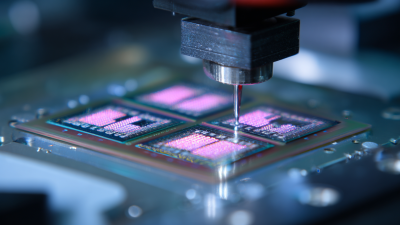
Wafer testing is a critical process in the semiconductor industry. It ensures the quality and performance of electronic components. Effective wafer testing can prevent issues in later manufacturing stages. Skilled technicians must understand various testing methods. Failures caught early through precise testing save both time and resources.
The reliability of wafer testing directly impacts product performance. A well-structured testing process can identify flaws in chips before they reach customers. Each test should be carefully designed, focusing on specific parameters. Deploying advanced testing technologies can enhance accuracy significantly. However, the process is not immune to challenges. Sometimes, tests do not yield clear results, necessitating careful analysis and adjustments.
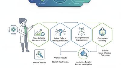
Continued refinement in wafer testing techniques is essential. New technologies can improve precision, yet human error remains a factor. It's crucial to remain vigilant and adaptable. Learning from past mistakes can lead to better testing processes. Emphasizing collaboration among engineers can drive innovation. Wafer testing is not just about following protocols; it’s about improving quality and reliability continuously.

Understanding the Importance of Wafer Testing in Electronics
Wafer testing is crucial in the electronics industry. It helps ensure the reliability and performance of semiconductor devices. According to a report by IC Insights, the global semiconductor market is projected to reach $1 trillion by 2030. This growth increases the demand for effective wafer testing processes.
Effective wafer testing identifies defects early. It prevents costly failures in later production stages. For example, a study by SEMI indicated that companies experience an average of 30% yield loss due to undetected defects. Early detection through rigorous testing not only saves costs but also boosts customer satisfaction.
The complexity of today's chip designs requires advanced testing techniques. Traditional methods may not suffice, and new technologies are emerging. These include electrical testing and optical inspection. However, many companies still rely on outdated practices. Regular review and updates of testing protocols can bridge this gap. Identifying the right balance between traditional and modern testing techniques is essential.
Essential Tips for Effective Wafer Testing in Electronics
| Test Method |
Description |
Importance |
Recommended Frequency |
| Electrical Testing |
Tests the electrical properties of the wafers, such as resistance and capacitance. |
Ensures functional integrity of the components. |
Every batch |
| Optical Inspection |
Analyzes the wafer surface for defects using optical methods. |
Critical for detecting physical defects. |
After each wafer fabrication |
| Mechanical Testing |
Assesses the mechanical properties, such as stress and strain. |
Helps in understanding material durability. |
Quarterly |
| Thermal Testing |
Evaluates how well the wafer can withstand temperature variations. |
Essential for reliability in high-temperature environments. |
Bi-annually |
| Cleanliness Testing |
Checks the wafer for contaminants that might affect performance. |
Ensures high yield and performance. |
Monthly |
Key Equipment and Tools for Wafer Testing Procedures
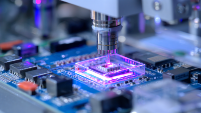
Wafer testing is a critical step in the semiconductor manufacturing process. Understanding the necessary equipment and tools can significantly enhance testing efficiency and accuracy. Key instruments include probe stations, test handlers, and automated test equipment (ATE). These devices help streamline the testing process and ensure high-quality outcomes.
For instance, probe stations allow engineers to make precise electrical contact with wafer circuits. This detailed measurement is vital for identifying defects at an early stage. Data from the Semiconductor Industry Association states that efficient wafer testing can reduce production costs by up to 30%. Understanding these tools can lead to improved defect detection and higher yield rates.
Always remember to calibrate your equipment regularly. Regular calibration helps maintain accuracy. Implementing a checklist of checks before running tests can save time and resources. Another tip is to consider ambient conditions. Temperature and humidity can affect results. Keeping an eye on these factors is crucial. Proper use of equipment and attention to detail can lead to more reliable data, allowing for better decision-making in the production process.
Essential Tips for Effective Wafer Testing in Electronics
This chart illustrates the average yield rates of various wafer testing techniques used in the electronics industry. The data highlights four common testing methods: Electrical Testing, Optical Inspection, Mechanical Testing, and Thermal Testing. Understanding the effectiveness of each method can guide improvements in wafer quality.
Common Wafer Testing Methods: Techniques and Best Practices
Wafer testing is crucial in electronics. Various methods ensure that wafers meet quality standards. Common techniques include
electrical testing, optical inspection, and various physical tests.
Each method offers unique insights into the performance of semiconductor devices.
Electrical testing checks the functionality of wafer chips. This involves applying voltages to detect any faults.
It's efficient but may overlook minor defects. Optical inspection, on the other hand, uses high-resolution imaging to spot surface irregularities.
This technique is effective but can generate false positives, leading to unnecessary rework.
Physical tests, such as delamination and adhesion assessments, can provide vital information on wafer integrity.
However, these tests are more time-consuming and require precise conditions. Employing a combination of these methods can lead to more accurate results.
It's essential to continuously evaluate and refine testing processes. Embracing improvements can reduce errors and enhance wafer quality.
Interpreting Testing Results: Metrics and Analysis
Interpreting testing results in wafer testing is crucial for the electronics industry. Metrics such as
yield, defect density, and
electrical performance provide insights into the manufacturing process. Understanding these metrics helps
engineers make informed decisions about quality control and design improvements.
Yield rates are particularly important. A high yield indicates a successful process, while a low yield
signals underlying issues. Examining defect density helps pinpoint specific problems in the production line. Electrical performance metrics show how well a
wafer meets the required specifications. Each of these metrics reveals different aspects of the overall testing results.
However, it’s not always straightforward. Anomalies can arise, leading to confusion in data interpretation. Engineers must be cautious and avoid jumping to
conclusions based on initial results. Revisiting the testing process and ensuring accurate measurements can improve reliability. Data should be contextualized
within the larger production framework to identify patterns. Embracing a reflective approach can
ultimately enhance testing effectiveness.
Troubleshooting Common Issues in Wafer Testing Processes
Wafer testing plays a crucial role in the electronics manufacturing process. However, it often comes with challenges. One common issue is variations in test results. When results fluctuate, it can indicate a problem with the wafer itself or the testing equipment. Conducting regular maintenance and calibration of testing tools is key. Consistency ensures accurate readings.
Another frequent issue is contamination on the wafer surface. Particles or residues can significantly impact performance. Cleanroom protocols must be strictly followed. Implementing rigorous cleaning processes can help maintain wafer integrity. Visual inspections can also aid in identifying visible debris before testing.
Lastly, inadequate test coverage becomes a concern. If certain areas of the wafer are not adequately tested, critical defects may go unnoticed. Utilizing advanced testing techniques can help address this. However, it requires continuous assessment of testing methods and technologies. Exploring new approaches can lead to improvements. It’s essential to remain open to refining processes based on outcomes.