Ultimate Guide to PCB Test Jig for Efficient Circuit Testing in 2025
In the rapidly evolving landscape of printed circuit boards (PCBs), the efficiency and accuracy of circuit testing have become paramount for manufacturers and engineers alike. As we look ahead to 2025, the role of PCB test jigs has emerged as a critical component in ensuring that circuits meet stringent quality standards and performance expectations. Renowned expert in the field, Dr. Emily Chen, emphasizes the importance of this technology by stating, "A well-designed PCB test jig not only streamlines the testing process but also significantly reduces the chances of errors, ultimately leading to higher product reliability."
The ongoing advancements in PCB test jig technology suggest a future where testing processes are increasingly automated and precise. With the rise of new materials and complex designs, the need for adaptable and efficient testing solutions has never been more pressing. In the coming years, manufacturers will turn to innovative PCB test jigs that can handle the nuances of modern circuitry, providing effective solutions for both prototype and mass production testing.
As we delve into the ultimate guide to PCB test jigs, we will explore the latest trends, design considerations, and the technological advancements shaping the future of circuit testing. Through this exploration, it becomes clear that investing in high-quality PCB test jigs is not just a strategic choice but a necessity for ensuring the success and reliability of electronic products in an increasingly competitive market.

The Importance of PCB Test Jigs in Electronics Manufacturing
In the rapidly evolving landscape of electronics manufacturing, the role of PCB test jigs has become increasingly crucial. These specialized tools are designed to facilitate efficient testing processes, ensuring that printed circuit boards (PCBs) meet stringent quality and performance standards. According to a recent report by the IPC—Association Connecting Electronics Industries, the global market for PCB testing is projected to grow at a compound annual growth rate (CAGR) of 5.4% by 2025, underscoring the critical need for efficient and reliable testing methods. Test jigs play a vital role in optimizing throughput while minimizing the risk of defects, which is essential in high-stakes environments such as aerospace and automotive sectors.
The importance of PCB test jigs extends beyond mere efficiency; they are pivotal in enhancing reliability and performance metrics of electronic devices. In a survey conducted by the IEEE, 78% of manufacturers reported that implementing robust testing strategies, including the use of specialized jigs, significantly reduced the rate of field failures. Furthermore, integrating automated testing facilities with advanced test jigs can lead to a 40% reduction in manual testing times. This not only accelerates the time-to-market for new products but also significantly reduces costs associated with rework and warranty claims. As manufacturers strive for excellence in their production lines, the innovative designs and functionalities of PCB test jigs serve as an indispensable asset in maintaining high standards of quality assurance.
PCB Test Jig Efficiency in Electronics Manufacturing 2025
This chart illustrates the efficiency of PCB test jigs in terms of error detection rates during the manufacturing process. The data reflects trends observed in the electronics manufacturing sector in 2025.
Key Features of Efficient PCB Test Jigs for 2025
In 2025, efficient PCB test jigs will be more critical than ever as the demand for high-quality electronics continues to rise. One of the key features of modern test jigs will be their adaptability to varying circuit designs. With the rapid evolution of technology, manufacturers need testing solutions that can accommodate different PCB layouts and functionalities. This adaptability not only improves testing efficiency but also reduces setup times, allowing engineers to focus on refining product quality rather than recalibrating their testing equipment.
Another essential feature of PCB test jigs in 2025 will be their integration with advanced software solutions. These systems will provide real-time data analysis and reporting, enabling quicker identification of potential defects. The utilization of artificial intelligence within these jigs will facilitate predictive maintenance, allowing manufacturers to foresee issues before they impact production. Additionally, enhanced user interfaces will simplify operator training, ensuring that teams can efficiently engage with the testing systems and interpret results effectively. Together, these advancements will signify a major leap in the reliability and efficiency of circuit testing processes.
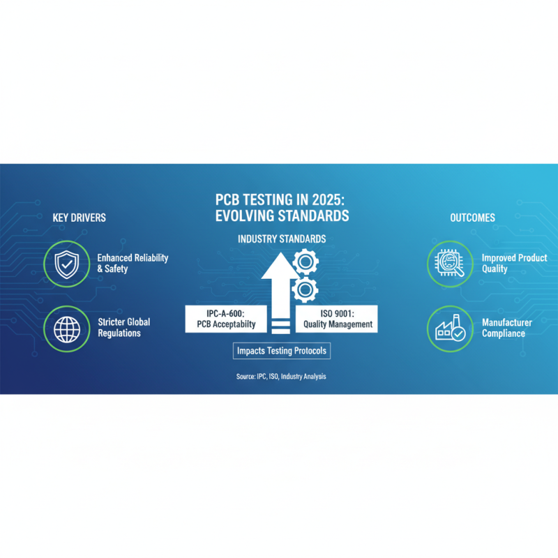
Industry Standards and Regulations Impacting PCB Testing
In 2025, the landscape of PCB testing will be significantly shaped by evolving industry standards and regulations that aim to enhance product reliability and safety. The international standards set by organizations such as IPC and ISO are becoming increasingly stringent. For example, IPC-A-600, which addresses acceptability of printed boards, outlines rigorous criteria for evaluating PCB quality and durability. Additionally, ISO 9001 certification is now often a prerequisite for manufacturers, ensuring adherence to quality management principles that ultimately affect testing protocols and outcomes.
Moreover, regulatory bodies are placing greater emphasis on environmental compliance, pushing organizations to adopt sustainable practices in their manufacturing processes, including PCB testing. The RoHS (Restriction of Hazardous Substances) directive, which limits the use of specific hazardous materials in electronic devices, necessitates that companies ensure their testing jigs comply with these environmental standards. A report by Market Research Future predicts that the global market for PCB testing is expected to reach $1.2 billion by 2025, driven by innovations in automated testing technologies that address these regulations. As such, companies will need to integrate these standards into their test jig designs to ensure compliance, efficiency, and reliability in their circuit testing processes.
Evaluating Cost-Effectiveness of PCB Test Jigs in Production
When evaluating the cost-effectiveness of PCB test jigs in production, manufacturers must consider several key factors that directly
impact their bottom line. The initial investment in test jigs can be significant, but this cost needs to be weighed against the potential savings achieved through increased
testing efficiency and reduced defect rates. A well-designed test jig can streamline the testing process, allowing for faster identification of issues and minimizing the
time spent on troubleshooting. This efficiency can lead to a lower overall cost per unit, especially in high-volume
production scenarios.
Another critical aspect is the long-term durability and maintainability of the PCB test jigs. A more robust jig may come with a higher upfront price, but
if it reduces maintenance costs and extends the lifespan of the equipment, it could prove more economical in the long run. Furthermore, evaluating the adaptability of
test jigs for different PCB designs can also enhance cost-effectiveness. Jigs that are easy to modify or reconfigure can
save precious resources by avoiding the need for an entirely new testing setup for each new product line. Thus, when assessing PCB test jigs, a holistic view of their
impact on production costs is essential for making informed investment decisions.
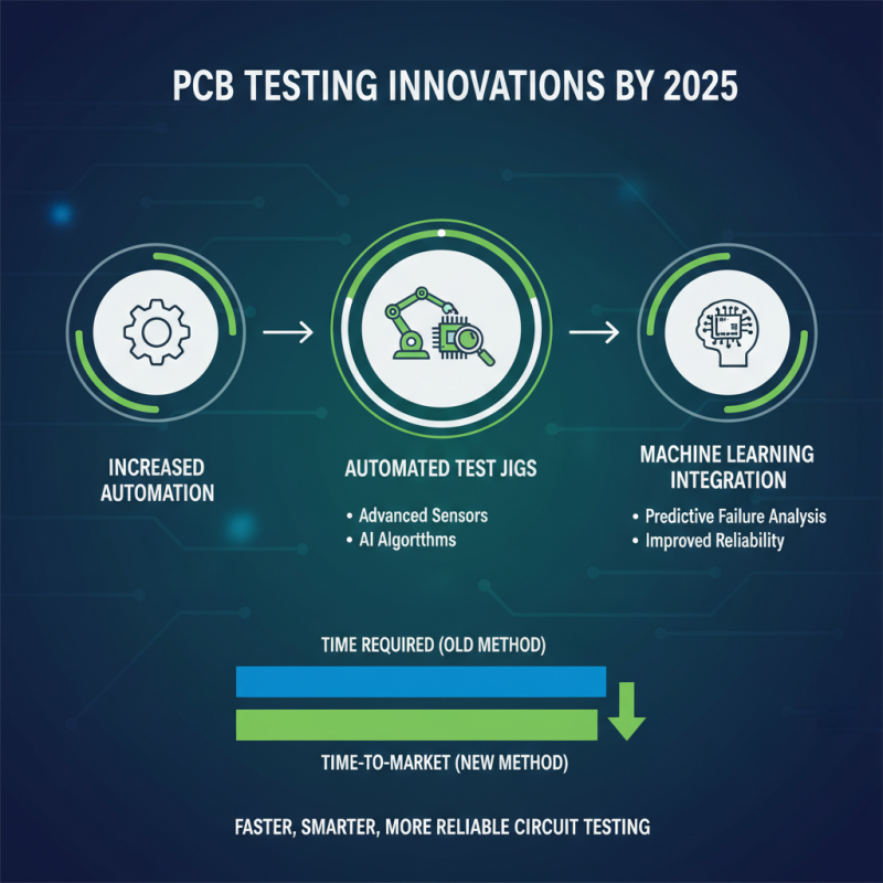
Future Trends in PCB Testing Technology and Their Implications
The landscape of PCB testing technology is evolving rapidly, with innovations set to reshape circuit testing methods by 2025. One significant trend is the increasing automation in testing processes. Automated test jigs equipped with advanced sensors and AI algorithms will not only enhance accuracy but also drastically reduce the time required for testing, leading to faster time-to-market for new products. Integrating machine learning will allow these jigs to analyze and predict potential failures, thereby improving reliability in the manufacturing process.
Another key development is the integration of IoT (Internet of Things) capabilities in test jigs. By leveraging connected devices, manufacturers can remotely monitor and manage testing procedures in real-time. This not only streamlines the testing process but also enables data collection for future optimization. The accessibility of data will provide engineers with insights into common failure points and design flaws, driving continuous improvement in PCB design and construction.
**Tips:** When choosing a PCB test jig, consider the future scalability of your testing solutions. Opt for jigs that can be easily upgraded to support upcoming technologies. Additionally, prioritize those that allow for easy integration with IoT platforms, ensuring a seamless transition into smart manufacturing workflows. Regularly updating your training on emerging testing technologies will also position your team for success in leveraging these advancements effectively.