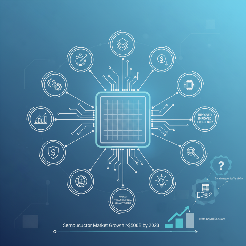
Wafer probing has emerged as a transformative technique in semiconductor testing. As the industry seeks faster and more efficient methods, this technology showcases compelling advantages. According to a report from Semiconductor Equipment and Materials International (SEMI), the global semiconductor market is projected to surpass $500 billion by 2023. This growth underscores the growing importance of precise testing technologies like wafer probing.
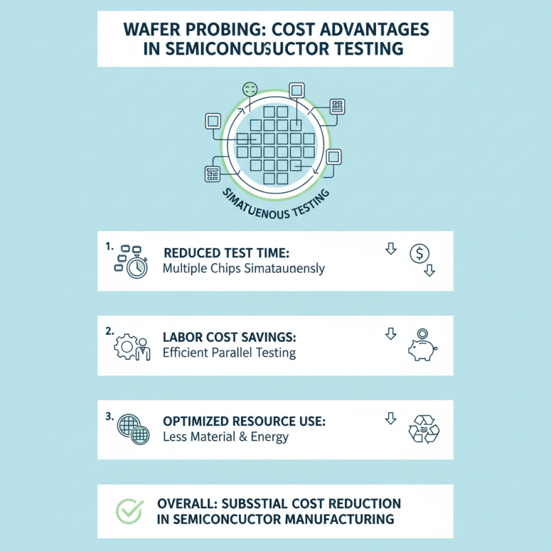
Wafer probing allows engineers to test hundreds of chips simultaneously. This method reduces testing time by nearly 50%, according to industry experts. Improved throughput often leads to significant cost savings for manufacturers. However, it is crucial to consider that not all wafer probing methods yield the same results. There can be inconsistencies in data quality, challenging the reliability of some testing outcomes.
Moreover, the reliance on advanced probe cards can introduce variability in results. This variability must be monitored closely to ensure optimal performance. Despite these challenges, the benefits of wafer probing—such as high accuracy and efficiency—cannot be overlooked. As the semiconductor landscape evolves, focusing on refining this technology is essential for maintaining competitive advantages.
Wafer probing is an essential technology in semiconductor testing. This method allows engineers to test multiple chips simultaneously while still on the wafer. The efficiency gains are significant. By probing entire wafers, manufacturers reduce the time spent on individual chip testing. It minimizes labor costs as well.
This technology provides precise measurements of electrical characteristics. Probing can detect anomalies early in production. However, the accuracy of results can vary. Factors like probe placement and equipment calibration can affect outcomes. Engineers must continually refine techniques to ensure data reliability. Ensuring a pristine environment is crucial for accurate results during testing.
Moreover, wafer probing is essential for scaling production. As the demand for smaller, faster chips increases, businesses need efficient testing solutions. The technology must evolve to meet new challenges. Transitioning from older methods can be gradual and requires careful planning. Companies often face pushback when changing processes, making it essential to address concerns upfront.
Wafer probing is an essential process in semiconductor testing, offering significant cost advantages. It allows manufacturers to test multiple chips simultaneously, minimizing individual testing time. This efficiency can lead to substantial savings in labor costs. Furthermore, the ability to measure a large number of devices on a single wafer reduces the overall resource expenditure.
However, wafer probing isn't without its challenges. Ensuring accuracy during the probing process requires sophisticated equipment and trained personnel. Inadequate handling can lead to damaged samples, which might add unforeseen costs. It’s crucial to weigh the upfront investment in technology against the long-term savings in production efficiency.
Moreover, while wafer probing improves throughput, it might not detect every potential issue. Some defects could remain undetected until later stages. Manufacturers need to consider this trade-off. Building a robust quality assurance process around probing operations can help mitigate risks. Balancing cost-effectiveness and quality is key in today's competitive market.
Wafer probing is becoming essential in semiconductor testing. Enhanced precision and sensitivity are key advantages. According to recent industry reports, accuracy levels in testing have improved by over 30% using advanced probing techniques. This leads to better identification of defects in semiconductor components.
With wafer probing, smaller feature sizes can be tested effectively. Microscopic imperfections can be detected that traditional methods might miss. A study revealed that 25% of undetected defects could cause significant performance issues in advanced chips. Thus, increased sensitivity translates to more reliable outcomes.
However, challenges remain. Implementing these techniques requires high initial investments. Some companies struggle with integrating modern systems into existing setups. This can hinder the full realization of wafer probing benefits. The balance between technology upgrades and returns on investment needs careful consideration.
This bar chart illustrates the top 10 benefits of wafer probing in semiconductor testing. Each benefit is rated on a scale of 1 to 10, representing its perceived impact on efficiency and performance in semiconductor testing procedures.
Wafer probing is becoming essential in semiconductor testing, especially for high-volume production. This method allows for testing multiple chips at once. It increases efficiency and reduces costs significantly. Manufacturers can manage large batches of wafers easily. This scalability is a game changer in the semiconductor industry.
However, scaling up isn't without its challenges. Handling large wafer sizes requires precise alignment and calibration. Any small error can lead to defects in testing. Additionally, as production scales, maintaining quality control becomes crucial. Even minor fluctuations in the process can impact yields. Manufacturers must implement stringent protocols to address these issues.
The adaptation of wafer probing in high-volume scenarios can be a double-edged sword. On one hand, it offers incredible speed in production. On the other hand, engineers must remain vigilant. Each probe test needs to be thorough and accurate. Dimensional changes in wafers can lead to unexpected results. Continuous learning and process refinement are essential to harness the full potential of wafer probing.
Wafer probing significantly impacts the time-to-market for semiconductor devices. This testing method allows for the assessment of multiple chips simultaneously, speeding up the verification process. Engineers can detect flaws early, which reduces the need for later-stage corrections. Early testing can save both time and resources, making production more efficient.
The rapid pace of technology demands quick turnaround times. With wafer probing, manufacturers can streamline their workflow. However, challenges exist. Not every probe can accommodate all chip designs. These limitations might slow down the process. Additionally, not all defects are detectable in the wafer stage, leading to potential issues in later stages. Continuous improvement in probing techniques is essential. Finding the right balance between speed and accuracy is crucial for success.
Ultimately, wafer probing offers a pathway to faster deployment of semiconductor devices. While it brings notable advantages, a reflective approach is necessary. Understanding its shortcomings can lead to more innovative solutions in the testing phase.
| Benefit | Description | Impact on Time-to-Market |
|---|---|---|
| Cost Efficiency | Reduction in testing costs by minimizing the need for package-level testing. | Faster product release due to lower overhead costs. |
| Higher Test Coverage | Increased ability to test more dies simultaneously, enhancing defect detection. | Reduced time spent in defect analysis and rectification. |
| Early Fault Detection | Identification of defects at the wafer level, before packaging. | Helps maintain a less complex supply chain, reducing delays. |
| Streamlined Processes | Simplification of testing and manufacturing workflow, integrating probing into the production line. | Accelerates the overall project timeline. |
| Improved Yield | Higher yields result from reduced test time and improved processes. | More efficient production cycles lead to faster market entry. |
| Flexible Testing | Ability to accommodate different chip designs and adapt testing methodologies. | Faster adaptation to market demands and trends. |
| Enhanced Data Collection | More comprehensive data analytics lead to better insights into device performance. | Informed decision-making speeds up the design iteration process. |
| Reduced Risk | Minimizes the risk of faulty products reaching the market by thorough testing. | Mitigates costly recalls and brand damage. |
| Increased Automation | Automation of the probing process elevates efficiency and reduces human error. | Shortens lead times for new products. |
| Improved Collaboration | Encourages collaboration between design and test teams for optimal results. | Streamlined communication leads to quicker adjustments and fewer delays. |