Top Trends in Semiconductor Test Sockets for 2025 You Need to Know
As the semiconductor industry continues to evolve, the role of semiconductor test sockets becomes increasingly vital in ensuring the integrity and performance of semiconductor devices. Experts in the field, like Dr. Emily Chen, a renowned semiconductor engineer, emphasize this importance by stating, "The efficiency of semiconductor test sockets directly impacts the ability to deliver high-quality products in today's fast-paced market." With innovation driving advancements in chip design and manufacturing, it is essential to stay abreast of the latest trends shaping semiconductor test sockets for 2025.
In the upcoming years, we anticipate significant developments in the design, materials, and functionalities of semiconductor test sockets. These trends not only reflect the growing complexity of semiconductor devices but also address the rising demand for improved testing solutions that facilitate faster and more reliable testing processes. Understanding these emerging trends will be crucial for engineers and companies striving to maintain a competitive edge in a rapidly transforming landscape.
This article will delve into the top trends in semiconductor test sockets that industry professionals must know for 2025, exploring the implications of these advancements on testing efficiency and semiconductor performance. By examining these trends, stakeholders can better prepare for the challenges and opportunities that the future holds in semiconductor testing technology.

Emerging Materials in Semiconductor Test Sockets for 2025
The semiconductor industry is poised for significant advancements in test socket technology, driven by the emergence of innovative materials as we look toward 2025. As devices become increasingly complex and miniaturized, the need for high-performance test sockets that can accommodate the evolving requirements of semiconductor testing has never been greater. Reports from industry experts forecast a continuous shift towards advanced materials, including ceramics, polymers, and engineered metal alloys, which offer improved thermal conductivity, reduced wear, and elevated precision in contacting.
With the rise of 5G, AI, and IoT applications, test sockets must not only support higher frequencies but also enhance reliability under extreme conditions. Emerging materials, particularly those that exhibit lower thermal expansion and higher elasticity, will play a crucial role in ensuring consistent performance. Recent market analyses indicate that materials such as liquid crystal polymer (LCP) and thermally conductive silicone are expected to gain substantial traction, owing to their efficacy in dissipating heat and maintaining structural integrity under pressure.
Tips: When selecting test sockets for next-generation applications, consider materials that offer both mechanical strength and thermal management capabilities. It’s beneficial to keep an eye on ongoing R&D in high-frequency applications, as this will impact the availability and development of new materials. Collaborating with material scientists can also provide insights into potential custom solutions tailored to specific testing environments. Adapting early to these material advancements could provide a competitive edge in achieving longer device longevity and improved accuracy in testing outcomes.
Advancements in Socket Design for Enhanced Testing Accuracy
The advancements in socket design are pivotal for achieving enhanced testing accuracy in semiconductor applications. As the complexity of semiconductor devices continues to increase, the demand for precision in testing has never been greater. Modern socket designs are incorporating innovative materials and engineering techniques to reduce contact resistance and improve signal integrity. This ensures that the tests conducted are reflective of the device's true performance, reducing the risk of faulty chips reaching the market.
Moreover, the integration of smart technologies within test sockets is paving the way for real-time data analysis during testing procedures. These intelligent sockets can monitor parameters such as temperature and humidity, providing critical insights that can influence the testing outcomes. By enabling adaptive testing methodologies, advanced sockets are enhancing not just accuracy, but also the efficiency of the overall testing process. As we approach 2025, these trends in socket design are set to transform how semiconductor testing is conducted, leading to more reliable and high-performing electronic components.
Automation Trends Shaping the Future of Semiconductor Testing
The semiconductor testing industry is undergoing a significant transformation driven by automation trends, which are expected to shape the future landscape of semiconductor test sockets by 2025. According to a recent report from the IPC (Institute for Printed Circuits), the adoption of automated testing equipment is projected to increase by 35% over the next few years. This paradigm shift not only enhances efficiency but also addresses the growing complexity of semiconductor devices, which are increasingly utilized in advanced applications like AI and IoT.
The rise of Industry 4.0 has brought forth enhanced capabilities in semiconductor testing through integrated automation solutions. As reported by SEMI, automated test equipment (ATE) utilization is set to expand, with over 60% of semiconductor manufacturers implementing automated test sockets to streamline operations and reduce human error. These advancements allow for more accurate data collection and faster turnaround times, enabling businesses to meet escalating market demands while maintaining high standards of quality assurance.
Moreover, the integration of artificial intelligence and machine learning algorithms in testing processes is revolutionizing the industry. A study by McKinsey highlights that companies implementing AI in their testing protocols see a reduction in test cycle times by up to 50%. This not only accelerates product development cycles but also significantly reduces operational costs, allowing companies to allocate resources toward innovation and development of next-generation semiconductor technologies.
Impact of Miniaturization on Test Socket Development
The ongoing trend of miniaturization in electronic components is significantly influencing the development of semiconductor test sockets. As devices become smaller and more powerful, the demand for compact test solutions that can accommodate tight geometries has surged. According to a recent report by Mordor Intelligence, the global semiconductor test equipment market is expected to grow by over 10% annually, with miniaturization being a primary driver of this growth. This shift necessitates the evolution of test sockets that can seamlessly integrate with smaller device footprints while ensuring accuracy and reliability in testing processes.
To address the challenges posed by device miniaturization, manufacturers are focusing on innovative designs and materials for test sockets. Advanced materials such as LCP (Liquid Crystal Polymer) and new plating techniques are becoming increasingly prevalent, providing the necessary thermal and electrical performance in reduced dimensions. Research from the Semiconductor Industry Association (SIA) indicates that nearly 70% of semiconductor firms are prioritizing miniaturization in their testing strategies, pushing for developments that allow for high-density packaging and complex assembly. These innovations not only enhance performance but also improve manufacturability and yield rates, which are critical factors in meeting the growing market demand for high-performing, compact electronic devices.
Top Trends in Semiconductor Test Sockets for 2025 You Need to Know
| Trend |
Description |
Impact on Testing |
Projected Growth (%) |
| Miniaturization |
The reduction of socket size to accommodate smaller chips. |
Increases flexibility in design and integration into compact devices. |
15% |
| Advanced Materials |
Utilization of new materials for better heat dissipation and electrical performance. |
Enhances accuracy and reliability of testing. |
20% |
| Integrated Solutions |
Development of sockets that integrate test and handling functions. |
Reduces cycle time and increases throughput in testing. |
25% |
| Automated Testing |
Adoption of automation in the testing process for efficiency. |
Minimizes human errors and accelerates testing speed. |
30% |
| Sustainability Focus |
Emphasis on eco-friendly materials and processes. |
Aligns testing processes with global sustainability goals. |
10% |
Sustainable Practices in Semiconductor Test Socket Production
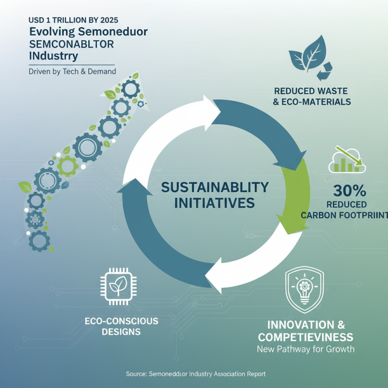
As the semiconductor industry continues to evolve, sustainable practices in semiconductor test socket production are becoming increasingly imperative. The global semiconductor market is projected to reach USD 1 trillion by 2025, driven by advancements in technology and rising demand for electronic devices. According to a recent report by the Semiconductor Industry Association, the shift towards sustainability is not just a regulatory response but a new pathway for innovation and competitiveness. Production methods that minimize waste and utilize environmentally friendly materials are gaining traction, with companies investing in eco-conscious designs that reduce their carbon footprint by up to 30%.
Moreover, industry analysts predict that by 2025, sustainable manufacturing practices will significantly influence consumer preferences, with 67% of professional buyers indicating they prefer suppliers who adhere to green practices. This transition is impacting the design and development of test sockets, which are crucial for ensuring the reliability and performance of semiconductor devices. Green initiatives such as the use of recyclable materials and energy-efficient manufacturing processes not only align with environmental goals but also enhance product lifecycle management, making the semiconductor testing more efficient and cost-effective. Ultimately, as sustainability becomes a focal point, the future of semiconductor test sockets is set to embrace innovative practices that contribute to both economic and environmental resilience.