Semiconductor demand is expanding, but every untested die remains a potential production loss. The World Semiconductor Trade Statistics (WSTS) Autumn 2024 Forecast projects global semiconductor sales will reach $626.9 billion in 2024 and $697.2 billion in 2025. These figures highlight a simple pressure: manufacturers must improve output without compromising reliability. Wafer probing provides the first electrical checkpoint before wafer dicing and packaging.
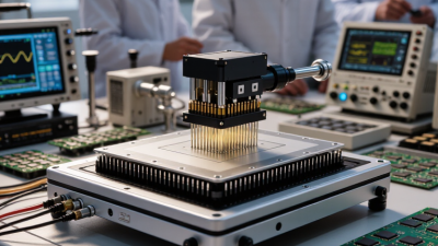
During wafer probing, a probe card contacts tiny aluminum or copper pads across each die. Automated test equipment applies controlled signals, measures electrical responses, and records pass or fail results. Engineers use these results to identify defective dies, map wafer-level yield, and protect later assembly stages from avoidable costs. That makes yield visible. It also creates traceable data for process control.
The SEMI Global Wafer Fab Forecast continues to track substantial worldwide fab capacity growth, increasing the need for consistent in-line testing. More wafers mean more test data, not merely more production volume. In practical operations, probe-mark depth, contact resistance, alignment accuracy, and temperature can influence results. A small contact issue may resemble a device defect. No probe card is perfect. This is where experienced engineers review distributions, retest rules, and abnormal wafer maps rather than trusting one measurement blindly. A simplified explanation can mislead. Still, the central value of wafer probing is clear: it prevents known electrical failures from moving downstream, supports reliable binning, and strengthens evidence for manufacturing decisions. Understanding this stage explains why semiconductor testing begins long before a packaged chip reaches the customer.

Wafer probing is the electrical checkpoint between wafer fabrication and final semiconductor packaging. It tests thousands of individual dies while they remain on a 200–300 mm wafer. A probe card touches tiny bond pads, applying controlled signals and measuring voltage, current, leakage, timing, or resistance. Each die receives a pass, fail, or performance classification.
This process protects time and materials. Packaging a defective die can add unnecessary cost and hide problems until much later. Probe data also creates a wafer map, showing patterns across the surface.
A cluster of failed dies may indicate contamination, uneven deposition, lithography variation, or temperature effects. Engineers compare these maps with process records to locate recurring defects. The measurements must remain stable, because contact resistance or a damaged probe can create misleading results.
In production environments, technicians control alignment, pressure, cleaning, and test temperature carefully. A 300 mm wafer offers high die density, but it also increases mechanical and data-handling demands. Testing speed matters, yet excessive speed can reduce measurement confidence. It is a difficult balance.
Wafer probing is not flawless. A passing result does not guarantee lifetime reliability, and a single test condition cannot represent every operating environment. Some failures appear only after packaging or extended stress. For that reason, engineers review probe results alongside inspection, reliability, and yield data. Careful probing does not remove uncertainty, but it reveals weak dies before they consume more resources.
Why Is Wafer Probing Important in Semiconductor Testing?
At 40–100 μm pitches, wafer probing becomes a precision problem, not a simple contact step. The probe card must land on tiny pads without bending, sliding, or damaging fragile structures. The 2023 IEEE Heterogeneous Integration Roadmap identifies 40–100 μm interconnect pitches as a practical challenge for advanced packaging. That range leaves very little mechanical tolerance.
Each probe needle or vertical contact carries test signals from automated equipment to the die. Engineers measure leakage current, contact resistance, continuity, threshold voltage, and high-speed response. A poorly aligned contact can look like a defective chip. That is the uncomfortable part.
Contact force matters. Too little force creates unstable readings. Too much force can mark the pad or shorten probe life. Temperature adds another variable. During high-current tests, local heating may change resistance and distort results. Industry guidance from SEMI emphasizes controlled wafer-level test conditions, including repeatable contact and measurement environments.
Probe cards also manage thousands of electrical paths at once. The 2024 IEEE Heterogeneous Integration Roadmap links higher interconnect density with tighter signal-integrity and thermal constraints. In practice, this means calibration cannot be treated as paperwork. It must be checked across wafers, temperatures, and repeated touchdowns. Some test limits remain imperfect, especially when tiny pitch, contamination, and probe wear interact. That uncertainty deserves measurement, not assumptions.
A wafer probe test checks each die before it enters assembly. Fine needles touch tiny contact pads while the tester applies electrical patterns. The resulting wafer map marks dies for packaging, rework, or rejection. This early gate matters because a weak die can consume a package substrate, bonding time, and assembly capacity before failing at final test. That is expensive. The hands-on detail matters: a probe mark, contact resistance, or unstable test result can change a die’s classification.
The scale is substantial. SEMI’s 2024 materials report valued the global semiconductor packaging materials market at $23.5 billion in 2023. That figure is not a measure of avoidable waste, but it shows the resources downstream processes handle. Screening defective dies before packaging can help preserve those resources and keep assembly lines focused on usable units. Probe data is not a crystal ball. Poor contact or an overly strict limit can misclassify a good die, so teams review test limits and correlate probe results with final-test outcomes. The map may look clean; the edge dies still deserve a second look.
Wafer probing checks electrical behavior before individual dies are packaged. Fine needles contact tiny pads on the wafer, while test equipment measures properties such as leakage, resistance, and operating speed. Each tested die receives a result linked to its position on the wafer. With thousands of dies, that location matters as much as the pass or fail label.
Engineers can turn these measurements into wafer maps and compare patterns across production lots. A cluster of weak dies near one edge may point to a process or equipment issue, while scattered failures can suggest a different problem. Trends in test values can also reveal dies that pass today but sit close to a rejection limit. Probe data helps narrow investigations; it does not prove the root cause by itself. Contact quality, temperature, and test coverage can all affect the picture. Real data is sometimes messy.
Tips: Keep test conditions consistent and record them with each wafer map. Review both failure locations and measurement ranges, and check unusual patterns against repeat tests before changing a process. A neat map can still mislead.
Wafer probing takes place while dies remain on the intact silicon wafer, before dicing separates them. A probe card’s tiny needles touch each die’s contact pads. The tester checks electrical behavior, such as leakage, continuity, and basic function. Results become a wafer map, marking dies for later handling. A red mark on one die can spare it a costly trip through packaging.
That timing matters. Dicing turns the wafer into individual chips; packaging then adds connections and protection. Known-good-die screening helps avoid spending those steps on chips that already fail electrically. It is useful, but not magic. Probing cannot fully reproduce the heat, physical stress, or system conditions a packaged device may encounter. Final testing remains necessary.
The scale of the work is reflected in industry forecasts. SEMI’s October 2024 equipment forecast projected global test-equipment sales of $7.7 billion in 2024 and $9.8 billion in 2025. WSTS’s Spring 2024 forecast put worldwide semiconductor sales at $611.2 billion for 2024. Those figures describe broad markets, not wafer probing alone. Still, they show why catching defects early can matter across high-volume production. A wafer map also has limits: probe contact can vary, and borderline results may need review before a die is discarded.
Why Is Wafer Probing Important in Semiconductor Testing? - Where Wafer Probing Fits Before Dicing, Packaging, and Final Testing
| Manufacturing Stage | What Happens | What Is Tested or Recorded | Why It Matters | Typical Outcome |
|---|---|---|---|---|
| Wafer fabrication complete | Integrated circuits have been formed across the wafer, but the individual dies have not yet been separated. | Wafer identification, lot information, process history, and test-program setup are verified. | Establishes traceability and confirms that the wafer is ready for electrical testing. | The wafer is queued for probe testing. |
| Wafer probing | A wafer prober positions each die beneath a probe card. Probe needles contact the die’s test pads while automated test equipment applies signals and measures responses. | Electrical checks may include continuity, leakage, voltage or current behavior, timing, memory functions, and other device-specific tests. | Finds electrically defective dies while they are still on the wafer, before the cost and handling involved in dicing and packaging. | Each tested die receives a pass, fail, or other test classification. |
| Wafer map and yield review | Test results are associated with die locations and assembled into a wafer map. | Pass/fail locations, test bins, recurring failure patterns, and wafer-level yield are reviewed. | Shows where usable dies are located and can help identify patterns that may point to process or equipment issues. | Passing dies can be identified for downstream handling; failing dies can be excluded or specially marked. |
| Dicing | The wafer is cut into individual dies, commonly using a sawing or other separation process. | The wafer map and die identification data guide selection and tracking of individual dies. | Probe results help avoid spending downstream effort on dies already identified as electrically defective. | Dies are separated for assembly or other disposition. |
| Packaging | Selected dies are assembled into packages, with electrical connections made between the die and package terminals. | Assembly records and die traceability are maintained; packaging itself is not a substitute for wafer-level electrical testing. | Wafer probing provides an early screen, while packaging protects the die and enables connection to a circuit board or system. | Packaged devices proceed to post-assembly testing. |
| Final test | Packaged devices are tested using package contacts and production test equipment. | Device-specific electrical functions and applicable production limits are checked; testing may also cover behaviors not fully assessed at wafer level. | Confirms device performance after assembly and can detect issues introduced or revealed during packaging. | Devices are classified for shipment, rework where applicable, or rejection. |
| How wafer probing and final test work together | Wafer probing tests the die before separation; final test evaluates the assembled device after packaging. | Results from both stages support yield monitoring, defect analysis, and product quality control. | Neither stage fully replaces the other: probing screens dies early, while final test checks the completed packaged product. | A staged test flow helps make manufacturing decisions throughout production. |
Note: Test coverage and limits vary by device type, process, and manufacturing flow. Wafer probing can identify many die-level electrical failures, but it does not guarantee that a packaged device will pass final test.