What Is a Test PCB and How Is It Used?

A test PCB is more than a bare board with test points. It is a practical tool for checking whether a circuit behaves as designed, from power-up to final inspection. Engineers use it to measure voltages, trace signals, verify component placement, and reveal faults before they spread into a larger production run. A probe touching a labeled pad can uncover a weak connection. A repeatable fixture can expose a failure that visual inspection misses. Small details matter.

Quality expert W. Edwards Deming is often associated with the reminder, “Without data, you’re just another person with an opinion.” That principle applies directly to test PCB work: useful measurements turn assumptions into evidence. Deming was not a PCB specialist, so his words are a quality principle, not a quotation about test boards specifically. In practice, engineers must still question their results. A board can pass one test and fail under heat, vibration, or a different load. No single measurement tells the whole story.

This guide explains what a test PCB is, how engineers design and use one, and which methods help produce dependable results. It also considers common limitations, including poor probe access, unclear labeling, and test points placed too close together. The goal is not to promise perfect boards. It is to show how careful testing can make problems easier to find, understand, and correct. Short checks matter. A reliable process begins with clear questions and repeatable measurements.
What Is a Test PCB and How Is It Used?

What Is a Test PCB and What Does It Do?

A test PCB is a printed circuit board built to check whether an electronic assembly works as intended. Unlike a standard product board, it may include accessible test points, jumper links, or sockets for measurement. These features let technicians examine voltage, current, signal timing, and continuity without probing tiny component leads. Small details matter. A misplaced test point can slow the process or produce inconsistent readings.

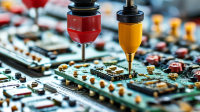
During evaluation, the assembly under test is connected to the test PCB or held against it with a fixture. In-circuit probes contact selected pads, while instruments record electrical behavior during defined operations. The board can also route power, simulate inputs, or connect sensors and communication ports. Results help reveal open connections, incorrect component values, shorts, or signals that fall outside expected ranges. It is useful for prototypes and repeatable production checks. Still, a test PCB does not prove every possible operating condition. Its coverage depends on test-point placement, measurement limits, and careful setup. That part is easy to underestimate.

What Parts and Features Make Up a Test PCB?

A test PCB combines the circuit under evaluation with features that make measurement repeatable. Typical parts include test pads, connectors, component footprints, routed traces, and a ground plane. Test pads expose specific signals to probes; their spacing must match the fixture or handheld probes. Connectors bring power and signals onto the board. Fiducial marks help align automated inspection equipment. Keep it measurable. IPC-2221 provides design guidance for spacing and layout, while IPC-9252 addresses electrical testing of unpopulated boards.

Some boards also include isolation slots, current-sense resistors, or boundary-scan connections, depending on the test plan. A 2024 Grand View Research report valued the global PCB market at USD 73.53 billion in 2023; that figure shows the industry’s scale, not a universal test-board specification. Not just copper. In practice, engineers should label test points clearly and leave room for probe access. A dense layout can look elegant but make troubleshooting awkward. That trade-off is easy to miss. Review the board with the actual fixture, test limits, and measured signals in mind, then revise where access or readings prove unreliable.

What Is a Test PCB and How Is It Used? — Parts and Features

Part or Feature What It Is How It Is Used Typical Design Consideration
Printed circuit board (PCB) An insulating substrate with conductive copper traces, pads, and other patterned features. Provides the mechanical support and electrical connections for the test circuit or device under test. Choose a suitable board material, layer count, thickness, and copper weight for the signals and test conditions.
Device under test (DUT) footprint A set of pads or holes laid out to match the package and pin arrangement of the component or assembly being tested. Connects the DUT to the test circuit, socket, or measurement equipment. Match the footprint to the component package and verify pin numbering, pad dimensions, and orientation.
Test points Accessible pads, plated holes, or connectors placed on electrical nodes of interest. Allow probes or leads to measure voltage, current, or signal activity during testing. Provide enough clearance for the intended probe and label important measurement nodes clearly.
Connectors and headers Interfaces such as pin headers, terminal blocks, or board-edge connectors. Connect the test PCB to power supplies, instruments, fixtures, or other boards. Check pin assignment, current capacity, voltage rating, and mechanical orientation.
Power and ground connections Traces, planes, pads, and connectors that distribute supply voltage and provide return paths. Deliver power to the DUT and establish a reference for measurements. Size conductors for expected current and use a suitable return-path layout to limit voltage drop and noise.
Signal-routing traces Copper paths that carry signals between the DUT, test points, and interface components. Route stimulus and response signals through the test circuit. For fast or sensitive signals, consider trace impedance, path length, spacing, and return-current continuity.
Passive components Components such as resistors, capacitors, and inductors fitted to the board. Set bias conditions, filter noise, limit current, or provide loads and termination for a test. Select component values and ratings appropriate to the circuit and test limits.
Protection components Components such as fuses, current-limiting resistors, or transient-suppression devices. Help reduce the risk of damage from overcurrent, incorrect connections, or electrical transients. Choose protection levels that suit the expected operating range without interfering with the intended measurement.
Jumpers and configuration links Removable shunts, solder bridges, or switches that alter circuit connections. Enable test options such as selecting a signal path or disconnecting a circuit section. Document each setting and make selectable configurations easy to identify.
Silkscreen markings Printed legends on the PCB, typically showing reference labels, polarity, pin names, or instructions. Help users connect, probe, configure, and inspect the test board correctly. Keep labels legible and avoid placing them where components or connectors will obscure them.
Mounting holes and alignment features Mechanical features used to secure or position the board in an enclosure or test fixture. Keep the PCB stable and help align it with probes, sockets, or other equipment. Check hole size, edge clearance, fastener access, and fixture alignment before fabrication.
Test fixture or socket interface A board area or connector arrangement designed to mate with a fixture, socket, or probe system. Supports repeatable connections when testing multiple components or assemblies. Verify contact spacing, insertion direction, mechanical tolerances, and expected cycle life.

How Is a Test PCB Designed for a Device?

A test PCB is designed around the device’s real operating conditions, not just its schematic. Engineers begin by listing the signals, power levels, connectors, and measurements the board must support. They also check the device’s size and mounting points. For a compact handheld unit, even a few millimeters can determine whether test probes reach the pads.

Test points are placed where technicians can access them without touching nearby components. Their labels should be readable, and sensitive signals may need short routes or shielding from noisy power traces. Protection components can help prevent accidental shorts during repeated measurements. Small details matter. The layout is then reviewed for clearance, grounding, and compatibility with the test fixture. A crowded connector can make a sound circuit frustrating to test.

Before fabrication, engineers verify the schematic and inspect the board layout against the device requirements. They may use simulation or design-rule checks, but neither replaces testing a physical board. Measurements on an assembled prototype can reveal unexpected noise, voltage drops, or probe access problems. The first layout is rarely perfect. A test point may sit beneath a fixture edge, or a cable may pull at an awkward angle. Revising the layout after these observations makes the next version more reliable and easier to use.

How Is a Test PCB Used to Check a Circuit?

What Is a Test PCB and How Is It Used?

How Is a Test PCB Used to Check a Circuit?

A test PCB provides a practical way to inspect a circuit under controlled conditions. It may include test pads, connectors, and components arranged for easy probing. The board can represent an early design or hold a circuit being checked during production. Clear labels help a technician locate power, ground, and signal points without guessing.

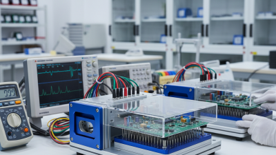
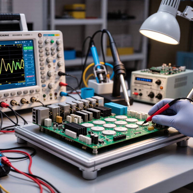
Testing usually begins with a visual check for solder bridges, misplaced parts, or damaged traces. With power disconnected, a multimeter can check continuity between selected points. Then apply the specified supply voltage, preferably with a current limit set to protect the circuit. Measure key voltages at test pads and compare them with the design values. An oscilloscope can reveal unstable signals or unexpected noise. Small errors matter. If a reading is wrong, check probe contact and ground connection before changing components. A single pass is not proof that every circuit condition works; testing only the easiest points can miss faults.

Tips: Record the expected and measured values beside each test point. Use short probe leads for cleaner signal readings. Power down before moving connections. A neat test setup helps, but it cannot replace checking how the circuit behaves during real operation.

Where Are Test PCBs Commonly Used?

Test PCBs are commonly used in electronics labs, production facilities, and repair workshops. Engineers use them to check circuit behavior before approving a design or assembling larger quantities. Labeled test points provide access to voltage, signal, and ground connections. A technician can place a probe on a clear pad instead of balancing it against a tiny component lead. That makes measurements easier to repeat.

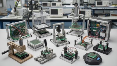
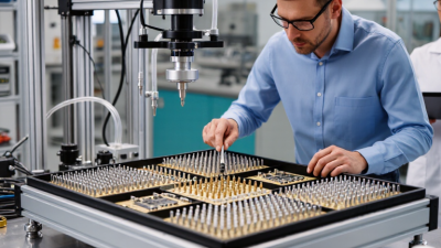
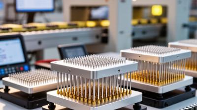
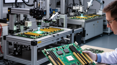
On production lines, a test PCB may connect a device to an automated fixture. Spring-loaded pins touch designated pads while the system checks power, communication, or sensor responses. This can reveal assembly faults early. But it is not foolproof. Worn fixture contacts, incorrect limits, or a mismatched board revision can lead to misleading results.

Test PCBs are also useful during prototyping, component evaluation, and product troubleshooting. For example, a technician might compare a regulator’s output under load with its expected range. Small details matter. Teams sometimes notice only after repeated use that a test point is hard to reach. That deserves review: a test PCB can improve measurement access, but careful setup and sound circuit design still matter.

Go to Top