Choosing a wafer probing service can affect more than test speed. It can influence measurement quality, engineering decisions, and the time needed to resolve device failures. A capable provider should explain how its equipment fits your wafer size, pad pitch, probe card, and test conditions. Ask whether the setup supports the required temperature range, contact force, and electrical measurements. Details matter.
The service’s process deserves the same attention as its equipment. Look for clear procedures for calibration, wafer handling, test-program review, and lot traceability. Ask what data you will receive, how results are organized, and whether engineers can help investigate unexpected readings. A sample report or trial run can reveal practical issues, such as inconsistent contact marks or missing fields, before a larger lot is tested. Ask for evidence.
Price and turnaround time matter, but neither tells the whole story. Compare quotes against the actual scope of work, including setup fees, retesting, data delivery, and support when results look unusual. No checklist is perfect. A provider may appear suitable on paper yet struggle with a particular device or schedule, so leave room for a technical discussion. This guide outlines the questions that help you compare wafer probing services with care, weigh trade-offs, and choose a partner whose capabilities match your project rather than relying on broad promises.

How to Choose a Wafer Probing Service?
What a Wafer Probing Service Does
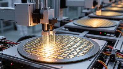
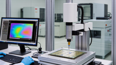
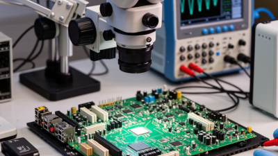
A wafer probing service checks electrical performance before individual chips are packaged. A precision prober brings tiny probe-card needles into contact with pads on each die. Test equipment then applies signals and measures responses, such as leakage current, resistance, or operating speed. The results help engineers identify dies that meet defined limits and flag possible process issues. Each tested die can be recorded on a wafer map. This makes the data easier to review alongside production records. The service may also support tests at different temperatures when a device’s requirements call for them.
Good probing depends on more than making contact. Alignment, probe-card condition, contact force, and test settings can all affect readings. A poor contact may look like a device failure; repeated marks on pads may also deserve investigation. Ask how the provider verifies test setup, handles questionable results, and reports retests. Clear answers matter. A neat wafer map is useful, but it cannot explain every anomaly by itself. Engineers should review the underlying measurements before drawing firm conclusions.
Tips: Share device limits, pad layouts, and temperature needs early. Request sample reports. Check how failed or inconsistent measurements are reviewed, not just how quickly testing is completed.
Wafer probing makes electrical contact with individual dies on a wafer so their devices can be tested before packaging. This illustrative MOSFET output-characteristic sweep shows how drain current changes with drain voltage at several gate voltages. Actual measurements depend on the device design and test conditions.
A wafer probing service should match the measurements your device actually needs, not just offer a standard DC test. For logic and analog chips, check continuity, leakage, threshold voltage, on-resistance, and breakdown testing. These reveal open contacts, excess current, and weak structures before packaging. For RF devices, ask whether the setup measures S-parameters at your required frequencies. Power devices may need high-voltage or high-current testing, with suitable safety limits and temperature control. Small details matter: probe-tip force, pad pitch, and wafer edge exclusion can affect repeatability.
The wafer itself sets more requirements. Confirm support for its diameter, thickness, bow, and material, including silicon, SOI, silicon carbide, or gallium nitride. Ask how the service handles temperature sweeps and fragile or uneven wafers.
SEMI reported 12,602 million square inches of silicon wafer shipments in 2023, down 14.3% from 2022. That changing volume is a reminder to check capacity and turnaround, not assume them.
A neat specification sheet can still hide gaps. Request sample test data, calibration records, and a clear retest policy. I would not treat “compatible” as proof; ask for results on a wafer with similar pads and materials.
How to Choose a Wafer Probing Service?
How to Assess Probe Technology and Equipment
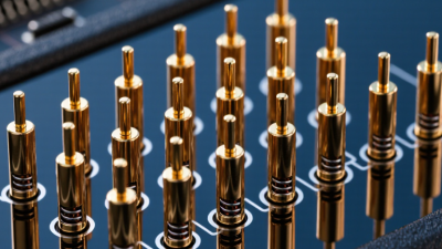
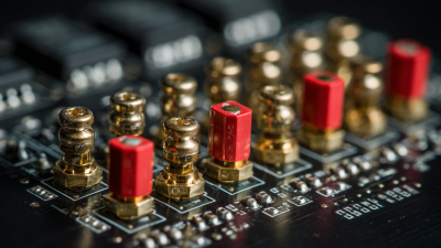
Probe technology should match the device, not just the quoted throughput. Check whether the service can handle your wafer diameter, pad pitch, current range, and test temperature. Ask how it controls probe-card alignment and contact force. A poor touchdown can leave scrub marks or create intermittent contact, especially on fine-pitch pads. Small details matter. Request repeatability data, contact-resistance records, and examples from comparable wafer structures. Look for measurements across wafer center and edge, not a single favorable site. For hot testing, ask how long the chuck stabilizes before readings begin.
Equipment investment offers context, not proof of service quality. SEMI reported that global semiconductor test-equipment sales rose 20% in 2024, reaching $8.2 billion in its Year-End 2024 equipment report. That growth signals continued investment in test capacity, but it cannot tell you whether one probing setup fits your process. Ask for a sample test report, including retest rates, alignment checks, and failed-contact handling. If possible, run a small engineering lot and compare results with your own reference measurements. Probe-tip wear can shift results over time; ask how often tips are inspected and what triggers replacement. A tidy specification sheet is reassuring, but raw logs often reveal more. Even then, one trial may miss an edge case.
A wafer probing service should be judged by records, not polished claims. For quality, request probe-to-probe repeatability, calibration history, contact-resistance limits, and retest rates for similar devices. Ask how wafer-sort results are correlated with final test, and how edge-die anomalies are flagged. Ask for proof. A useful sample report lists temperature, touchdown count, bin definitions, and timestamps.
Capacity is more than the number of testers on a website. Request weekly available slots, recent schedule attainment, backup equipment, and probe-card availability for your wafer size and pad pitch. SEMI’s Silicon Manufacturers Group reported 2023 silicon wafer shipments of about 12.6 billion square inches, down 14.3% from 2022. That industry swing is a reminder that market conditions change; it does not prove any single provider has spare capacity. Confirm a realistic ramp plan using your own lot size and turnaround target.
Compare total cost per accepted die, not just the quoted price per wafer. Include setup, engineering time, retests, data handling, and shipping. Ask for a written scope and sample output before committing. A low quote can age badly when exclusions appear. One caveat: a perfect audit checklist cannot predict every contact issue on a new layout. A small pilot lot can expose problems, though it adds time and cost.
When choosing a wafer probing service, ask for sample raw files, not only a polished yield summary. Match wafer IDs, die coordinates, test limits, units, and retest flags against the agreed test plan. Check that failed and retested die remain visible in the export. Small details matter. SEMI’s April 2024 year-end equipment report put 2023 global semiconductor equipment sales at $106.3 billion, down 1.3% from 2022. That figure is not a measure of probing quality, but it shows the scale of investment behind wafer production. Clear, traceable test records help teams investigate costly discrepancies.
Review how the provider defines yield and handles missing or invalid measurements. Request a report sample with timestamps, probe conditions, wafer-level summaries, and a die map that matches the raw data. Confirm file formats, naming rules, revision control, and who approves changes to limits. A spreadsheet can look tidy and still hide a retest exclusion. Ask for the delivery terms in writing: turnaround time, start-point for the clock, shipment or data-transfer method, and notice requirements for holds or wafer-count mismatches. Agree on what happens when data fails validation. No template catches every edge case. It is worth documenting one awkward scenario before production begins.