What Are the Top Test PCB Types for Buyers?
Buying the right test PCB begins with a simple question: what must the board prove? Some boards verify bare-board continuity and insulation. Others support functional testing, boundary-scan checks, or high-speed signal measurements. The best choice depends on product volume, test coverage, and how quickly designs change.
Prismark’s 2024 PCB industry reporting estimated global PCB production value at about $73.9 billion in 2023, underscoring the scale of a market where reliable verification matters. That figure covers the wider PCB sector, not test boards alone. For buyers, the practical distinction is whether a test PCB uses flying probes for flexible, lower-volume work or a bed-of-nails fixture for repeatable production testing. A dense fixture can shorten cycle time, but its tooling cost and maintenance deserve scrutiny. Small contact pads, tight tolerances, and accessible test points matter on the factory floor.
Signal-integrity educator Dr. Eric Bogatin’s core principle is often expressed this way: “The goal of signal integrity is to get the signal from the driver to the receiver with acceptable quality.” It is a useful reminder that test access must not compromise the signal being measured. IPC guidance and manufacturer capabilities can help buyers assess test coverage, materials, and quality controls. Still, specifications alone do not guarantee a smooth test. A neat taxonomy helps, but real projects rarely stay neat. This guide compares the top test PCB types and the trade-offs buyers should check before ordering.
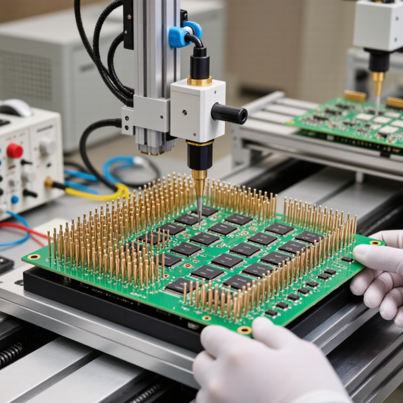
What a Test PCB Is and How It Supports Electronics Testing
A test PCB is a printed circuit board used to check whether an electronic assembly works as designed. It may be the board under test, or a purpose-built interface that connects a product to test equipment. Copper traces carry signals; test points give probes access to specific nodes. Some setups use a bed-of-nails fixture, while others use flying probes or boundary-scan methods. The choice depends on board volume, access, and the faults engineers need to detect.
A useful test PCB supports repeatable measurements without adding unwanted electrical effects. Engineers consider pad spacing, probe force, grounding, connector alignment, and signal integrity. For example, a poorly placed ground return can distort a high-speed measurement. That matters. A fixture should also allow easy replacement of worn probes and clear access to components needing rework. These details can be overlooked, especially when a design is rushed.
The wider industry context is growing quickly. The World Semiconductor Trade Statistics organization’s May 2024 forecast projected global semiconductor sales of $611.2 billion for 2024, a 16% increase over 2023. This is not a test-PCB market figure, but it illustrates the scale of electronics production that depends on reliable verification. A test board should match the product’s real operating conditions as closely as practical. Still, no fixture catches every fault; test coverage needs review against failure risks and measurement limits.
| Test PCB Type | What It Is | Typical Tests | Best Fit | Buyer Considerations |
|---|---|---|---|---|
| Bare-Board Test Coupon | A small PCB pattern manufactured alongside a production panel to represent selected board features. | Impedance, copper plating, trace geometry, and material-characterization checks. | Verifying that fabrication processes and controlled-impedance features meet design requirements. | Confirm that the coupon represents the relevant layer stack-up and trace geometry; it does not verify every feature on the finished board. |
| Flying-Probe Test Board | A finished PCB tested with movable probes that contact selected test points without a dedicated bed-of-nails fixture. | Electrical continuity and isolation checks, and detection of many opens and shorts. | Prototype runs, low-volume production, and designs that change frequently. | Usually avoids a custom fixture, but test time can increase with board complexity and the number of points to probe. |
| Bed-of-Nails Test Fixture | A PCB test setup that uses a custom fixture with spring-loaded probes contacting multiple board test points at once. | In-circuit checks such as connectivity, component presence, and selected component-value measurements. | Repeatable testing of stable designs in medium- or high-volume production. | Requires fixture design, manufacturing, and maintenance; the board must provide accessible test points and suitable mechanical clearance. |
| Functional Test Interface PCB | An interface board or adapter that connects a product PCB to test equipment and may route signals, power, or control lines. | Operational checks of assembled electronics, including selected inputs, outputs, and communication functions. | Production validation when a product needs application-specific electrical connections or test access. | Define connector mapping, signal limits, power requirements, and protection needs; functional coverage depends on the test plan and software. |
| Boundary-Scan Access PCB | A board layout or test-access design that provides connections to supported boundary-scan devices and their test signals. | Interconnect tests and selected device or board checks using boundary-scan circuitry. | Assemblies where physical probe access is limited and compatible devices are present. | Check that relevant devices support boundary scan and that the design exposes the required test-access signals. |
| High-Speed Impedance Test Coupon | A dedicated trace structure included in or associated with a PCB panel to measure controlled-impedance performance. | Characteristic impedance measurements on selected transmission-line structures. | Boards with high-speed signals or controlled-impedance requirements. | Specify the target impedance, trace structure, stack-up, and measurement method; coupon results represent the tested structure, not every signal path. |